
PCIe is an abbreviation for Peripheral Component Interconnect Express, an electrical interface standard used to connect high-speed add-in printed circuit boards (PCBs) to computer motherboards. GPUs, RAID cards, and SSD cards are all add-in cards. PCIE are found in many sizes: X1, X4, X8, X16, and X32. X1 stands for one Tx differential line and one Rx differential line.
You can use Ansys tools to design a motherboard or add-in board. You can use SIwave, HFSS, or 3D Layout. If your board contains PCIe lines, how do you know your design is correct? You need to check it against the PCIe specifications. So, we build, assemble, and test the PCB using well-known equipment. But this is a costly way. You would like to know if your design is acceptable while designing the PCB.
You can use the PCI template that OZEN Engineering developed to do that. The templates support PCIe1 to PCIe7 standards. If you open any one of them, you will find many circuits. Each circuit serves a purpose. Some of these have more than one circuit. All the necessary constraints, specifications, and limits are embedded in these circuits. We are talking about hundreds of numbers embedded in all these circuits. As we will see, these numbers are scattered in many places, but they are where they are supposed to be.
The circuits we have here are just the beginning, and users can construct an unlimited number of circuits based on them. Component The most important thing to remember is that all the necessary building blocks and setups exist in this Template; make a copy of them and run them.
Start first by generating the s-parameters of your model. In my case, I used SIwave to design and optimize a Motherboard. I solved 4 PCIe differential lines. These lines are RX lines. The Motherboard is supposed to support PCIe3 standards. You can also use measurements of some bare PCBs, i.e., with just traces and no components on them. You can do that also. The bottom line is that you need an S-parameter file.
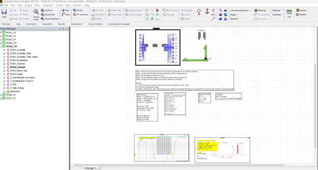 Figure 1: Circuit's contents
We come back to the Template. What will you find in each circuit?
The first thing you will notice is the information below the circuit.
- The first one is a detailed description of how to use the circuit.
- Second is some of the standards used in the circuit.
- Third is the preset setup for each Standard to be used in the circuit. We will talk more about it later on.
- The fourth is a list of the circuit's local variables and their descriptions. These are the local variables used in the circuit; changing them will only change this circuit. There are global variables. You will see them if you click on the name of the project. If you change these ones, it will change all the circuits in the Standard.
- At the bottom, you will find examples of the results. These are just pictures to demonstrate how the results should look. This is in case one of the graphs changes, and then the user can change it back to how it should look like.
We will discuss the circuit, the variables, and the results. The circuit contains an input, middle, and outer sections.
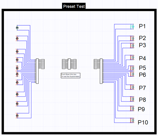 Figure 2: Circuit's structure
The input section contains all the possibilities for the source. Each possibility is represented by one eye source and one eye probe. The user can activate or deactivate any of them. The more circuits you activate, the longer the simulation takes, increasing exponentially. The input section has a switch that allows you to select which eye source/eye probe circuit to activate and which channel to test. If you have many channels, I am using 4 channels, so I am using a 4 channel switch. If you have 8 channels, you can use the one here.
The output section is the reverse of the input. It also has a switch so that you can select between channels and the different sources/probes. Each eye probe is connected to one eye source. The number of eye probes must match the number of eye sources.
How to control these channels and the circuits. We use the global variables list and adjust the channel number, Preset Case, or EqualizationCase numbers. We will talk more when we go through the circuits one by one. Click on the name of the Standard to see the global variables.
Why are we using the global variables and not the local variables to adjust subcircuits? Because the subcircuits cannot see the local variables of their own circuit, they can only see the global variables. So, if I have a local variable here, I cannot use it in any subcircuit. I can use local variables with the eye sources and eye probes, but not inside a subcircuit.
The middle section is the S-parameters. But it is not as simple as you think. Click on the middle block, and press Push Down. You will find the real circuit. The box in the middle is the S-parameters calculated using SIwave, HFSS, or 3D Layout. However, the S-parameters of the traces are not enough. You need to construct the rest of the structure. This picture for PCIe5 16GHz shows you the specifications of the PCIe5. It dictates that the loss of the Motherboard should not exceed 26.5dB. The package-on-die on the Motherboard should not exceed 8.5dB. The Add-in board loss should not exceed 9.5dB. The package-on-die of the Add-in should not exceed 4.2dB. All this information exists here. Notice that they call the Motherboard CBB, which stands for Compliance Base Board.
So, how do we use this information? Depends on what you are testing. Are you testing a Motherboard or an add-in board? Are you testing RX lines or TX lines? For example, in this video, we use the Motherboard's RX lines. Consequently, I need to add the loss of the Add-in board 9.5dB at the input and the loss of the package-on-die 4.5dB at the output. This full link should satisfy all the specifications.
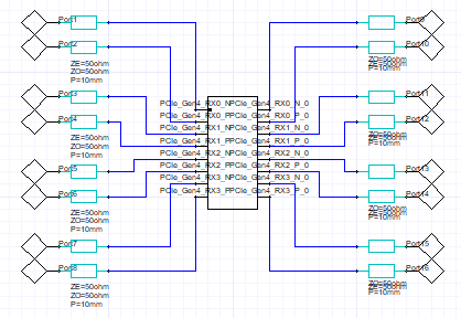 Figure 3: S-parameters and extra losses
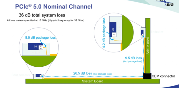
Figure 4: PCIe losses specifications
How to control these losses, using the global variables. If you go out of here by pressing Pop Up and selecting the Standard's name, you will see all the global variables. The ones you want to change are these attenuation variables. Because then they will apply to all the circuits of the Standard. So, I will enter 9.5dB for the input and 4.5dB for the output here.
Let us talk now about the variables. In each circuit, there are local variables that affect the eye sources and the eye probes. The definition of each variable is given in the Template.
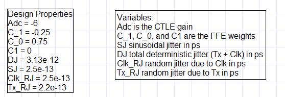 Figure 5: Local variables
If you open the eye source, you will see how they are used in the Bits, Jitter, and equalization panels. Again, they are local because the eye source can see them; they are only needed here.
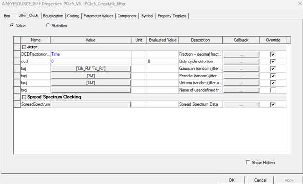 Figure 6: The use of the local variables (Jitters)
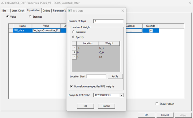 Figure 7: The use of the local variables for FFE
But there are global variables:
- First, the Vpp, which is the allowed peak-to-peak voltage.
- Second Tr the rising and falling time
- Third Bps, the data rate in bits per second, even if the signal is PAM4
- The channel number, the preset number, and the equalization cases. These are numbers used to control the input and the output switches.
- Finally, the attenuations are used in the middle sections.
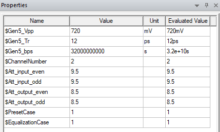 Figure 8: The global variables
If I open any eye source, you will see how these variables are being used.
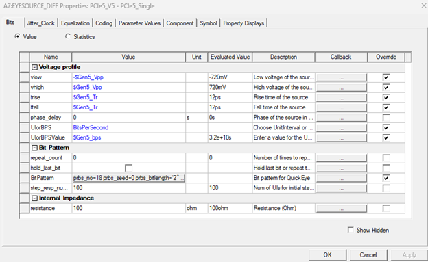 Figure 9: The use of the global variables
We will go through them again when we discuss each circuit.
For the results, the user will find four major types of plots:
- The eye width plot. It is simply a bathtub plot, and we use it to calculate the width of the eye and compare it against specifications. The user finds the limit line, the spec, the results, some instructions on reconstructing a similar plot, and finally, the Y-marker. The Y marker is fixed at y=1e-12 BER as per the spec of PCIE3. There is no direct way to calculate the delta of the Y-marker, so we are using a trick in the circuit tool to generate the curve you see here and use it to calculate the delta. This delta has to be bigger than the spec. The same spec is represented using the limit line. You may have one or many curves, and the Y-marker will show them all.
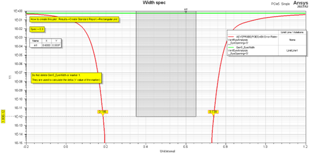 Figure 10: Bathtub and width specifications
 - The eye height eye plot is simply a contour plot of the BER values. Again, you will find instructions on constructing a similar one. You will find a delta marker that you need to move to touch the single contour plot that we have in the graph. We force the graph on the scale to have one contour at 1e-12 BER. Reading the delta of the eye tells if we are meeting the spec or not. In some standards, there is one eye because they use NRZ signals, but in PCIE6 and 7, we have three eyes because they use PAM4 signals. The spec is on the top eye. All that is programmed for the user.
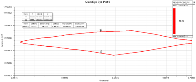
Figure 11: Height specifications - The third graph is the eye itself with respect to real-time in PS. The user can display the eye parameters by right-clicking and then selecting Calculate Eye measurements. None of these can be used against any specification. But they are good to know information. The longer the simulation duration, the more accurate the numbers the eye calculator calculates. You can control that time by clicking on the Quick eye setup, clicking on Select, new, and then generating a new setup. Notice that in the plot, we have the spec as a mask.
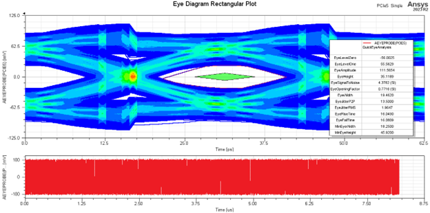
- Figure 12: Eye graph
Figure 13: Eye graph setup and options
- The second type of plot is the Eye diagram, but with respect to the unit interval. It is the same as the previous eye plot. Right-click and ask for the eye measurements. This time, all width measurements are in UI values.

Figure 14: Another eye graph - Return loss plot: This is another important plot that shows the return loss specification as a limit line. Notice also that the standards' specs are shown in the yellow box. There are differential and common mode return loss specifications.
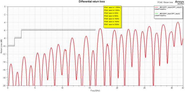
Figure 15: Return Loss
- The insertion plot: the differential insertion is part of the specifications but not the common mode insertion. Notice that there are two limit lines. The top one is for the Add-in card alone. The bottom one is for the full link. The information is given also in this small table.
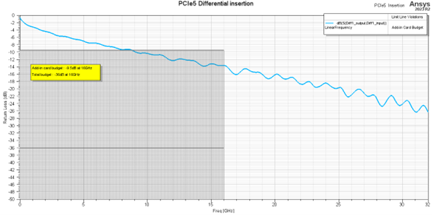
Figure 16: Insertion Loss
Let us start with the circuits one by one: First, the single case. This one has one eye source and one eye probe. It can be used to analyze one channel at a time. You can control the channel number using the global variable $Channel number. I can use this circuit to study some initial setups. I can also use the optimetrics to change the Vpp and the CTLE gain. You can also add another one for the channel or add the channel to the previous two. So, as you can see, the VPP and CTLE ranges are embedded in the optimetrics setup. These values are as in the specifications. From the results, we see the width, the height, and the eye plots. We also see the ones for the optimetrics setup. The first four are used when you do not use the optimetrics setup. Do not try to change that because you need the single set alone.
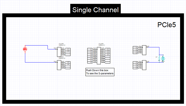
Figure 17: Single channel circuit
- The return loss and insertion setup: We talked about them before. Each circuit has the s-parameters and the switches. The user can change the $channel number or use it for the optimetrics. The structure uses the losses as per the global number for the return loss. These numbers are supposed to be common to all the circuits in the Standard. But for the insertion, the user can modify the attenuation using the local numbers inside the middlebox. You have to click here and Pushdown, and then you modify these numbers. So you can change them without affecting any other circuit in the Standard. You can study the effect of changing these attenuation numbers on the SI of the channels.
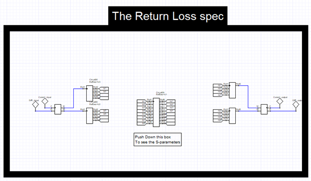
Figure 18: S-parameters circuit
- Preset: So, in PCIe, you can have some equalization. This equalization is done by adding FFE to the eye source, which stands for Feedforward equalization. In the Ansys circuit tool, you can leave them unspecified, and the circuit optimizes them. But according to the specifications, they have to follow one of 10 possibilities. To study all the possibilities, we used ten eye sources/ eye probes to represent each case. The FFE weights are usually given in the circuit diagram. The CTLE and the DFE are added to the eye probes. CTLE stands for continuous-time linear equalizer. It is just a driver with a peak at high frequencies to compensate for the loss in the circuit. The CTLE gain is a variable and can be changed from the local variable list. As per the specifications, the range of values allowed is found in the single-channel circuit. The DFE has a fixed number of tabs as per the specifications. The weights of these tabs are left to the circuit to optimize them. DFE stands for decision feedback equalizer. The FFE and DFE are mainly used to compensate for the memory of the channel. The memory is there because of the ISI and the poor transitions.
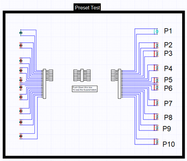
Figure 19: Single channel circuit
- The equalization setting allows the user to test the need for the three equalization options: FFE, CTLE, and DFE. Can we get away with two or just one of them? And what will each one of them contribute to the eye-opening? This is what this set will help you to study. Again, each case has it is own eye source and eye probe. The user needs to define the FFE parameters C_1, C_0, and C1 in the eye source. These values should match one of the ten possibilities mentioned in the preset test. The user can select which circuit to examine and on which channel to do the test.
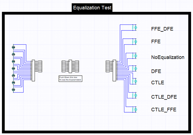
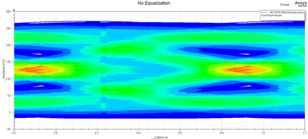
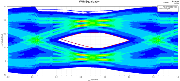
Figure 20: Eye with equalization
- The final set is the crosstalk/jitter and noise ones. This is where the eye is stressed with crosstalk, jitter, and/or noise. In each Standard, there are numbers that the user is forced to try. The stressed eye has to pass the spec (eye width and eye height). We have here three circuits, each circuit with specific capabilities. The jitter one has the Jitter numbers, so do not change them. The noise one has the jitter and the noise. You can deactivate the crosstalk in each circuit but do not change any other numbers, like the Jitter numbers or the noise problems.
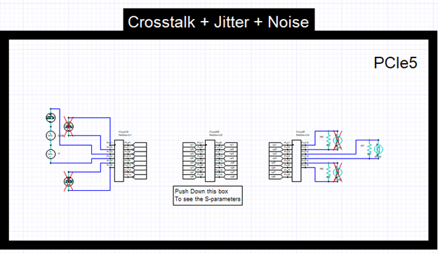 Figure 21: Crosstalk, Jitter, and Noise
So, using these circuits, the user can verify and optimize the design. The Template does not do any design or optimization but can ensure that the design meets the specification and by how much margin.
