
Discover the untapped potential of ANSYS simulation in optimizing optical lithography processes
Understanding Optical Lithography
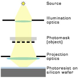
Optical lithography is a key process in the field of semiconductor manufacturing. It involves the use of light to transfer a pattern onto a photosensitive material known as a photoresist. This pattern is then transferred to subsequent layers of the semiconductor device to create the desired circuitry. Understanding the principles and intricacies of optical lithography is crucial for achieving high-quality and precise semiconductor devices.
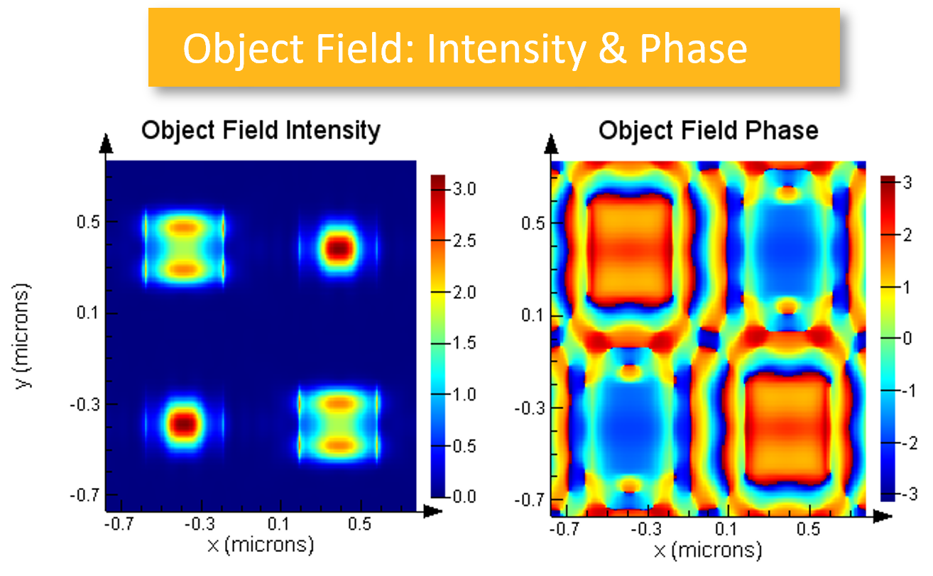
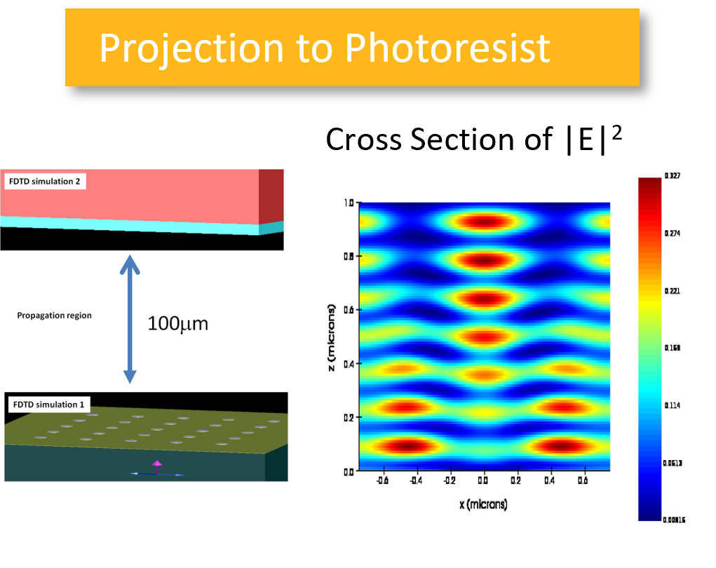
One of the main challenges in optical lithography is the ability to control the diffraction of light. As light passes through the various optical components, such as lenses and masks, it undergoes diffraction, which can distort the pattern being transferred. By simulating the behavior of light in the optical system, ANSYS simulation provides valuable insights into the diffraction effects and allows for the optimization of the lithography process.
Furthermore, ANSYS simulation also helps in understanding the impact of various process parameters, such as exposure time and dosage, on the final pattern quality. By analyzing different scenarios through simulation, engineers can determine the optimal settings for achieving the desired pattern fidelity.
In summary, a deep understanding of optical lithography is crucial for successful semiconductor manufacturing, and ANSYS simulation plays a vital role in optimizing the lithography process by providing insights into diffraction effects and process parameter optimization.
The Role of ANSYS Simulation in Optical Lithography
ANSYS simulation offers several benefits in the field of optical lithography. Firstly, it allows for the analysis and optimization of the optical system, including the lenses, masks, and other components. By accurately simulating the behavior of light, engineers can identify potential issues and make informed design decisions to improve the lithography process.
Secondly, ANSYS simulation helps in mitigating the effects of diffraction, which is a major challenge in optical lithography. By modeling the diffraction effects using advanced photonics simulation and evaluating different scenarios, engineers can develop strategies to minimize the distortion and improve pattern fidelity.
Additionally, ANSYS simulation enables the analysis of process parameters and their impact on the final pattern quality. By simulating different exposure times, dosages, and other variables, engineers can optimize the lithography process and achieve the desired pattern fidelity and resolution.
In conclusion, ANSYS simulation plays a crucial role in optical lithography by providing valuable insights into the behavior of light, mitigating diffraction effects, and optimizing process parameters for improved pattern quality.
Ozen Engineering expertise in optical lithography simulations
Ozen Engineering is a leading provider of ANSYS simulation services with expertise in optical lithography simulations. Our team of experienced engineers specializes in optimizing the lithography process for various semiconductor applications.
With a deep understanding of optical lithography principles and ANSYS simulation capabilities, we can help you overcome the challenges associated with diffraction, improve pattern fidelity, and optimize process parameters.
Whether you are looking to enhance the performance of your existing lithography process or develop a new process for advanced semiconductor devices, Ozen Engineering can provide the expertise and support you need.
Contact us today to learn more about our optical lithography simulation services and how we can help you unlock the untapped potential of ANSYS simulation.