
PCB Simulation
The increasing complexity of nowadays wireless RF devices increases the demand for accurate and efficient simulations of large and complex PCB designs. Identifying and predicting potential issues early in the design process saves resources, time, and money. SIwave helps you model, simulate and validate high-speed channels and complete power delivery systems typical in modern high-performance electronics. It accurately extracts multi-gigabit SERDES and memory buses, providing product sign-off compliance for various designs. SIwave’s full wave extraction of complete power distribution networks (PDN) enables you to verify noise margins and ensure impedance profiles are met through automatic decoupling analysis in low-voltage designs.
Overview
In this blog we will be using ANSYS SIwave tool to perform power integrity analysis based on DC IR simulation. The DC IR simulation of a PCB design allows the user to validate electrical performance by identifying regions of current crowding and high current vias. We will also show how to obtain tabular data for the current and resistance for the vias, and obtain loop resistance and inductance values.
DC IR Drop Analysis Setup
From the Quick Access Toolbar, we will open the SIwave workflow wizard, and then select Configure DC IR Drop Analysis.


The power nets show up in red color. From the list of Nets we will select the 1V0 net to run the simulation.
- Set U1 as a current source with 10 A
- And the U2 as a voltage source to 1.0 V
- Then click on Configure Simulation to apply pin groups and excitations to the design
- Click the Validate button, which brings up the Launch Validation Check window


The Validation Check analyzes the entire setup to ensure it is ready for simulation.
- Increase the Number of cores to use for this validation step by pressing the up button (arrow).
- Click OK to start the validation check.


Now we can click the Simulate... button. This brings up a Compute DC Current and Voltage Distribution window.

SIwave requires a global 0 Volt reference location. The zero-volt reference is automatically applied to the negative pin of the voltage source. This creates a reference point for voltage plots in the results.

Click the Other solver options... button. This brings up the SIwave Options tab dialog box.
In the SIwave Options window, in the DC tab:
- Choose Balanced
- The slider bar allows you to choose between three predefined settings. To see what settings are changed, move the slider bar to different positions and click on the DC Advanced tab.
- Also enable Compute Inductance to compute DC inductance along with resistance.

DC IR Simulation Results
After the simulation is done, we can see different types or results including:
- Currents/Voltages plot on planes and vias
- Loop resistance
- Current and Voltages report
- Power Tree
- RL and CG table
Currents/Voltages plot
In the Results window, under DC IR Drop Simulations, right-click on DC IR Sim 1 and select Plot Currents/Voltages

In the DC IR Drop Simulation Results window:
- Put check marks next to 1V0 power nets.
- Check the V check box only on the PWR layer to display the voltage plot on that layer
- You can as well click on J, Iv, and P
- Click Update Plot Display.
- Click Close to close the results setup window.

To turn off the view of this surface plot of voltage, click View >> Display Surface Plot as seen below.


Explanation of Via Currents, 𝑰_𝒗 :
- O and X represent current magnitude between layers.
- O is current to a layer towards the top of the stackup.
- X is current to a layer away from the top of the stackup.
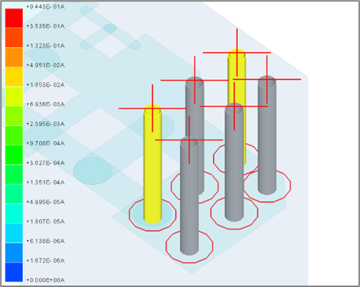
In this example, current is carried from layer TOP to BOTTOM through three vias. The red O and X represent a magnitude of current going between these two layers. In this case the magnitudes are not the same because some of the current supplied into the via from the TOP layer is distributed on other layers in the stackup and so less current travels out on the BOTTOM layer.
Loop Resistance
To view the Loop Resistance, Select Results >> DC IR DROP >> DC IR SIM 1 >> Loop Resistance Info


Power Tree
Select Results >> DC IR DROP >> DC IR SIM 1 >> Export Power Tree

Enter the Voltage Threshold and Current Threshold for all the components and Press OK


RL and CG table
From the Results window, under DC IR Drop Simulations, right-click on DC IR SIM 1 and select RL Table

This tables lists the R and L between the terminals defined in the design.

At the bottom of the window, enable (check) the option Display Self-terms only.
The video link below shows an illustration on how to do these steps in detail, and the model shown is available in the downloadable resources.
Downloadable Resources
SIwave Project