
Cutout sub-design in HFSS 3D Layout allows engineers to selectively extract and analyze specific sections within a PCB layout. This targeted approach accelerates simulations, streamlines complex computations, and enhances the overall efficiency of the design and analysis workflow. In this tutorial, I will demonstrate how to extract a portion of a PCB in HFSS 3D Layout using the cutout sub-design feature. Let's get started!
Overview
Let's consider the following PCB, which you can find in the examples folder: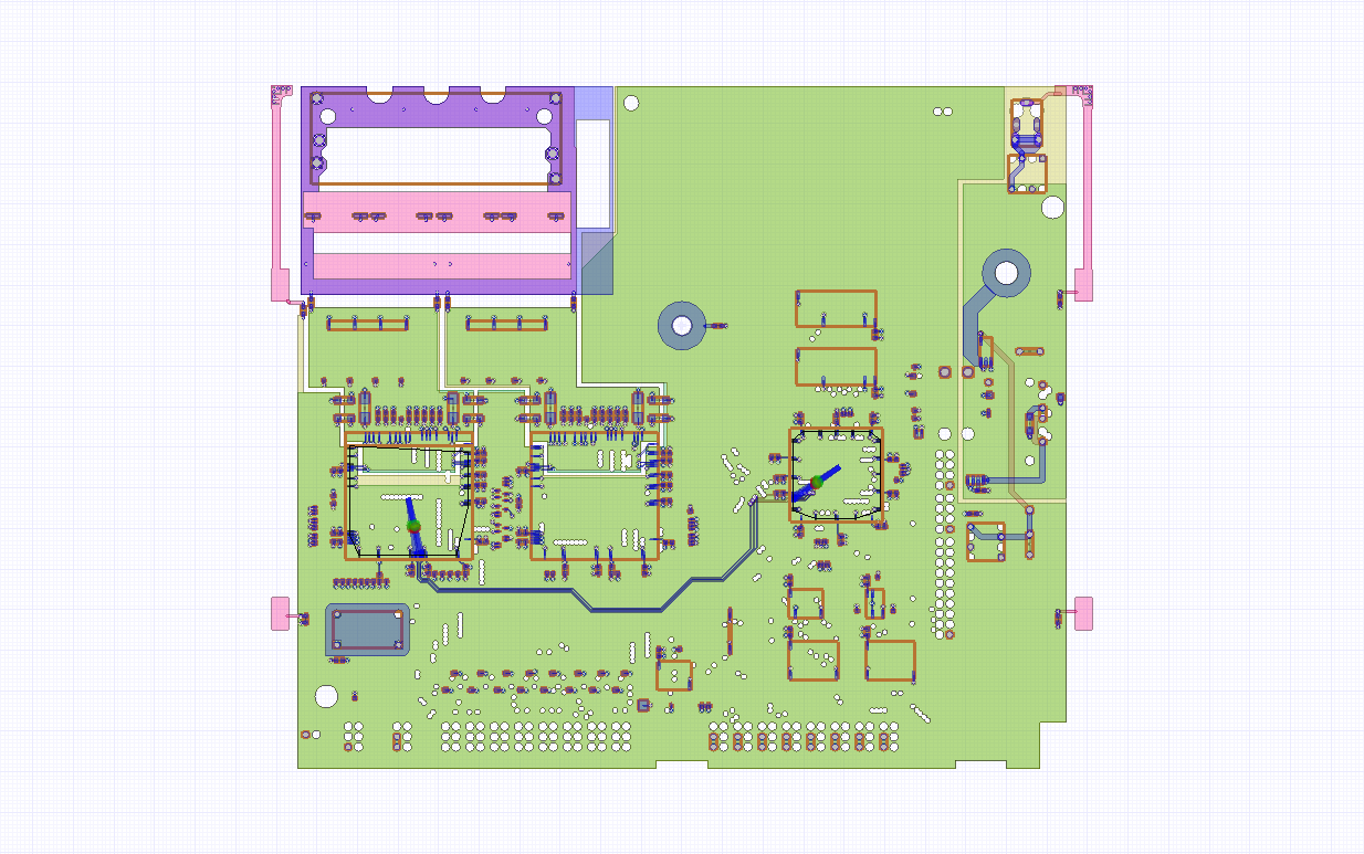
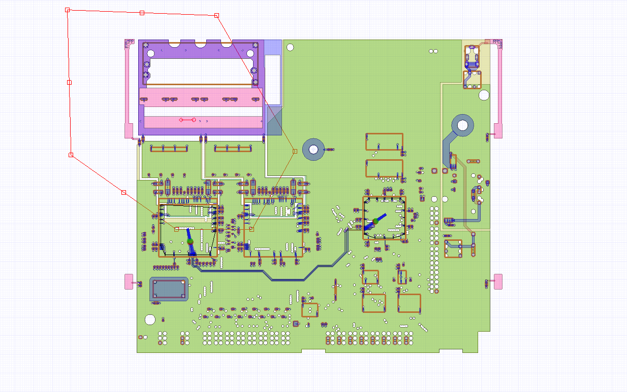
To begin, navigate to the "Layout" tab. Make sure the active layer is set to "Outline," which you can also achieve by selecting the radio button next to the "Outline" layer in the layers window.
Next, you need to draw a shape around the area you wish to extract; this shape will define the cutout region. For example, you can use a polygon tool to outline the desired section.
After defining your shape, click on "Cutout." This action opens the cutout sub-design window, where you have control over various cutout properties. You can choose to use the current design or create a new one by selecting "create new." Additionally, you can opt to create the cutout as a sub-design within the parent design.
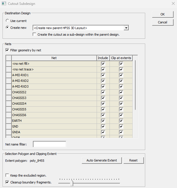
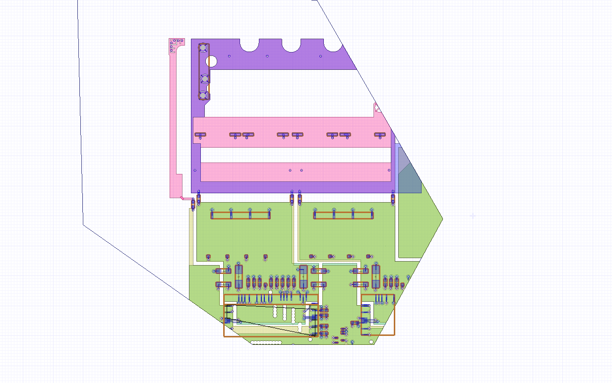
Once you have configured your cutout properties, click "OK" to complete the cutout. You will now observe a new design in the project manager. This newly created design encompasses the specific part of the PCB that you aimed to extract.
You can find the detailed demonstration just below: