Paul Dennig, Averatek Corporation
dennig@avertek.com, 408-310-6580
Mike Vinson, Averatek Corporation
mike@averatek.com, 215-264-0194
Mete Ozkar, Ozen Engineering Inc.
support@ozeninc.com, 408-732-4665
Chris Cowan, Ozen Engineering Inc.
cowan@ozeninc.com, 408-732-4665
Approach
For this work, we selected two target carrier frequencies: (i) 2.4 GHz (Bluetooth and WiFi) and (ii) 5.5 GHz (WiFi). At each frequency we designed three models, for six total antennas. At a given frequency, one antenna was a baseline model with a PCB laminate dielectric between the patch and the ground plane, the same laminate used for overall construction.
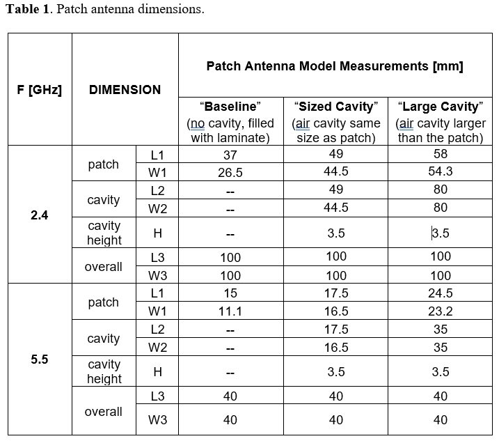
For the two experimental antennas at a given frequency, we replaced the dielectric with an air pocket in the shape of a rectangular parallelepiped (box). We began with the constraint that the height of a cavity would be the same as the dielectric that it replaced in the baseline unit. Keeping the internal height as a constant, we arrived at patches and overall antenna lateral dimensions that targeted the two carrier frequencies. The difference between the two experimental antennas at a given frequency was this: for one of those antennas, the air cavity was the same lateral size as the patch, and for the other model the air cavity was larger in extent than the patch, roughly 18 – 40% greater in a particular direction. The following Fig. 1 illustrates the three different types of antennas at a given frequency design point. A summary of all the antennas and their dimensions follows in Table 1.

Figure 1. The three patch antenna models: (a) baseline, (b) cavity same size as patch (“sized”), and (c) cavity larger than patch (“large”).
Procedure
The patch and ground copper thicknesses were standard 35.5 µm (“1 ounce copper “). For all models, the vertical distance between the patch and the ground plane was held to 3.5 mm. Figure 2 illustrates the sized antenna, highlighting the coaxial feed. The laminate FR-4 was used throughout this simulation study.
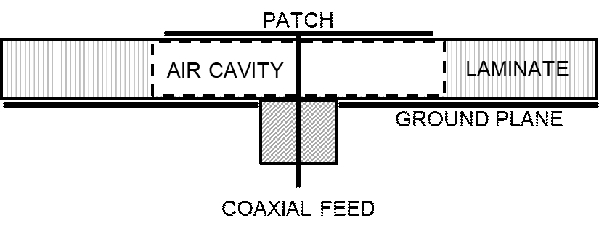
Figure 2. Side view of “sized” patch antenna model showing coaxial feed.
All antennas were simulated using Ansys™ HFSS software, operated by Ozen Engineering. All fabrication features, such as processing holes, 100 µm thin dielectric material over the patch, the SMA connector, and solid copper wire feed were all added to these models. A radiation box larger than the patch antenna was placed as a boundary condition with the patch antenna centered within. Automatic adaptive meshing was applied within HFSS to each scenario, using a medium curved surface setting. An example meshing is shown below in Fig. 3. Sensitivity analyses were attempted to help determine the large cavity size, however, the return loss showed little frequency variation with the large cavity, regardless of the target frequency.
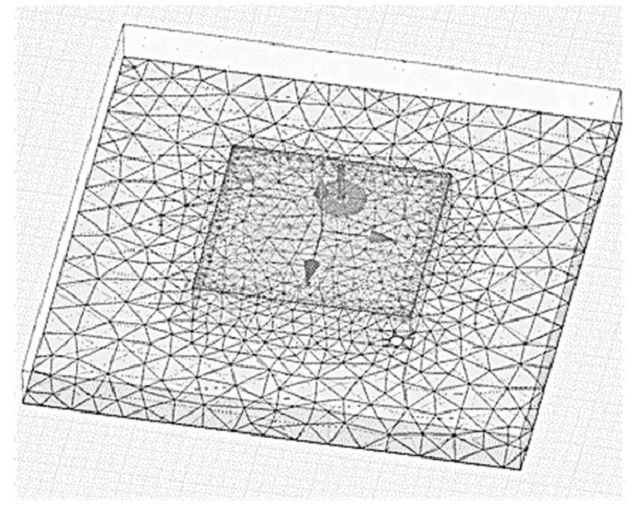
Figure 3. An example of the meshing of a patch antenna inside a fictitious radiation box using AnsysTM HFSS.
Data
We now present our simulation data. The simulated antenna gain, directivity, and radiation efficiency are summarized in Table 2 below.
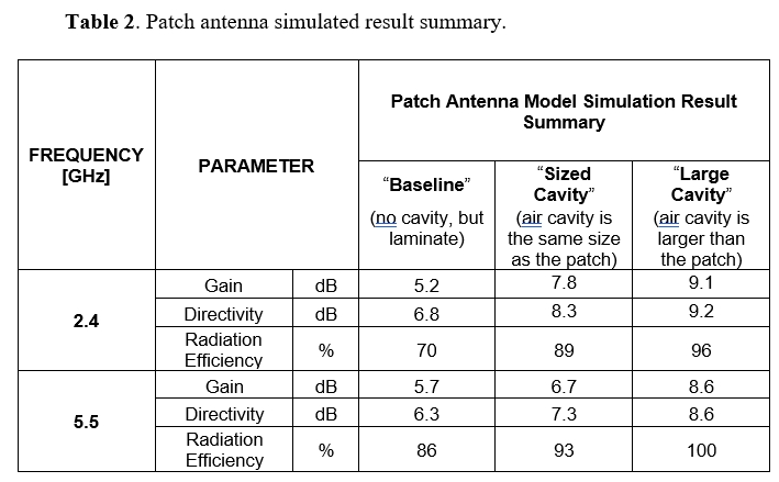
Figure 4 below shows the simulations of Return Losses superimposed, (a) is for the set of 2.4 GHz antennas and (b) is for the 5.5 GHz antennas. Within a set, the return losses were similar.
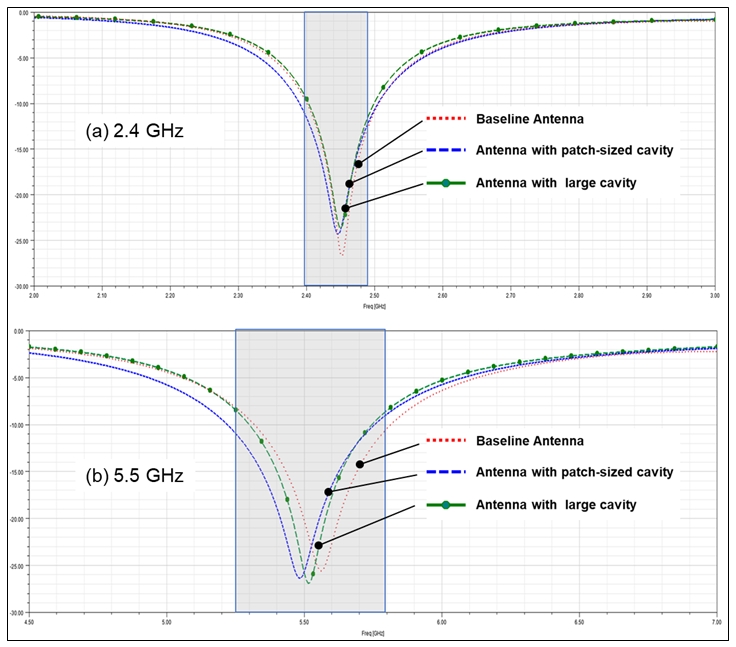
Figure 4. Simulated Return Loss [dB] versus frequency [GHz] for both sets of antennas, (a) 2.4 GHz and (b) 5.5 GHz. Within a set, the return losses were similar.
The Simulated Directivity is shown in Fig. 5 and the Simulated Realized Gain in Fig. 6, both below.
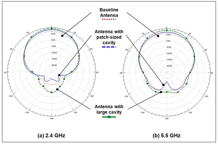
Figure 5. Simulated Directivity [dB] for (a) 2.4 GHz and (b) 5.5 GHz. Phi = 90°.
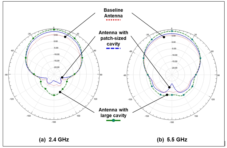
Figure 6. Simulated Realized Gain [dB] for (a) 2.4 GHz and (b) 5.5 GHz. Phi = 90°.
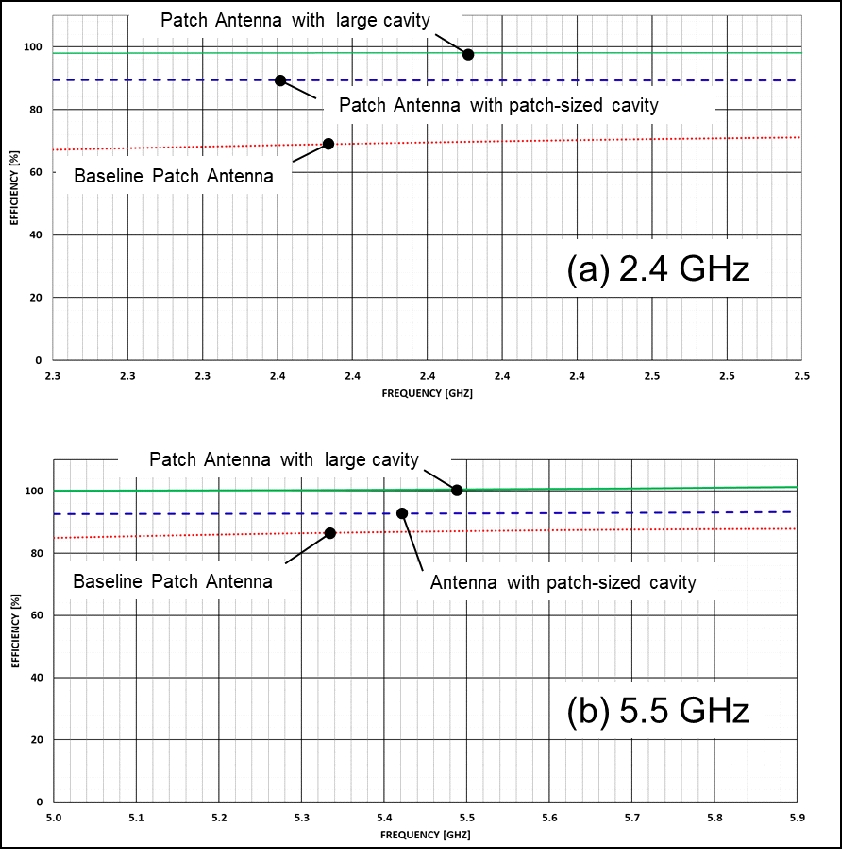
Figure 7. Simulated Radiation Efficiency [%] for (a) 2.4 GHz and (b) 5.5 GHz.
Figure 7 above illustrates the Simulated Radiation Efficiency for both design points. At both frequencies, efficiency improved dramatically with the increasing size of the air cavity.
Results and Discussion
At 2.4 GHz, the baseline patch antenna has a 70% radiation efficiency, while the patch antenna with patch-sized cavity has an 89% radiation efficiency. The patch antenna with the large air cavity has a 98% radiation efficiency.
At 5.5 GHz, the baseline patch antenna has an 86% radiation efficiency, while the patch antenna with the patch-sized cavity has a 93% radiation efficiency. The patch antenna with the large cavity approaches a simulated efficiency of 100%. The efficiency observed above 100% at the higher frequencies is due to numerical errors related to the radiation box that encloses the antenna. Making the mesh finer at the radiation box (smaller than λ/15) will fix this problem, as can be seen in the 2.4 GHz design. However, this approach takes a much longer time to solve for multiple frequencies and it is not generally recommended going forwards.
It is observed that the antenna with the cavity (same size as the patch) has a null in the Fig. 6 Realized Gain plot, which results in less back radiation.
Summary and Conclusions
Even though the bandwidth and directivity were similar in the different simulated configurations, there was a clear improvement in radiation efficiency when using an air cavity underneath the patch antenna (89% at 2.4 GHz design and 93% at 5.5 GHz) compared to the baseline patch antenna (70% at 2.4 GHz and 86% at 5.5 GHz). With the largest cavity antennas, the variations in width and length of the cavity in the sensitivity analyses did not affect the bandwidth and directivity a great deal. The efficiencies were even higher for the largest cavity antennas, compared to the other two configurations.
While we are confident in the efficiency simulation improvement trend as we moved from the baseline antennas with no cavity up to the largest air cavity models, we believe it is better to spend future efforts to obtain actual efficiency measurements to report our findings more accurately. The conclusion from the efficiency simulation study is that there are minimal losses for the case with the largest cavity.
The cavity overcomes the losses due to the dielectric substrate. These simulated efficiency differences are attributed to the dielectric losses in the baseline design, less so in the same-size-as-patch cavity stemming from the FR4 substrate material. When the air cavity was larger than the patch, the FR4 affected the efficiency the least. The measured efficiency of each actual manufactured antenna is expected to be slightly lower than what we found from simulation, due to the material properties and surface roughness of the patch copper which faces the internal ground plane, due to the skin effect.
This work represents an important finding, because the excellent efficiencies observed with the largest air-cavity patch antennas could realize a significant system power savings to achieve the same radiation power output. For example, reaching back through the system to the power amplifier, which is generally far less power-efficient than the antenna, would result in less power needed at the power amplifier. The impact could be realized in several ways, such as by extending the broadcast range, increasing the battery operation time, or by resulting in lower electromagnetic exposure to the equipment operator.
Future Work
During this writing, the antennas listed in Table 1 have been made using our proprietary construction techniques and they will all be evaluated on test equipment in an anechoic chamber shortly. We will compare the simulated responses of efficiency and directivity from the present study with actual measurements to be taken in our next study. An example of one patch antenna each from both the 2.4 GHz set and the 5.5 GHz set are shown in Fig. 8 below.
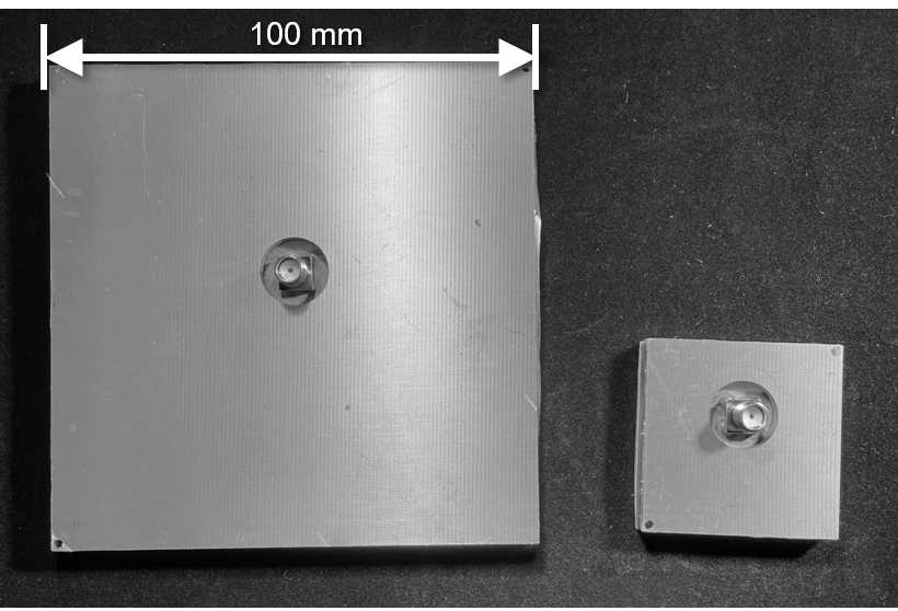
Figure 8. Fabricated patch antennas. Left: 2.4 GHz. Right: 5.5 GHz. The performance will be reported in a future work.
References
- Microstrip Patch Antennas, K.F. Lee and K.M. Luk, 2011 Imperial College Press, London.
- www.idc.com, 26 May 2021, “2021 Smartphone Growth to Reach Its Highest Level Since 2015, According to IDC”
- U.S. Patent, US10,862,220, Chi Lun Mak et al., Dec. 8, 2020.
Acknowledgements
Special thanks to Wuilbert Carreno, Maximus Kim, and Adrian Leenardo of Averatek for developing the processes to enable this line of work, assisting with the CAD, and for documenting the developments.
May 13, 2022 11:01:18 AM
