
PCB Simulation
The increasing complexity of nowadays electronic devices increases the demand for accurate and efficient simulations of electromagnetic compatibility (EMC) and electromagnetic interference (EMI). Identifying and predicting potential issues early in the design process saves resources, time, and money. ANSYS EMC plus enables the accurate simulation of printed circuit boards (PCBs), cables, and mechanical enclosures to help engineers in identifying likely problem areas and providing product sign-off compliance for various designs..
Overview
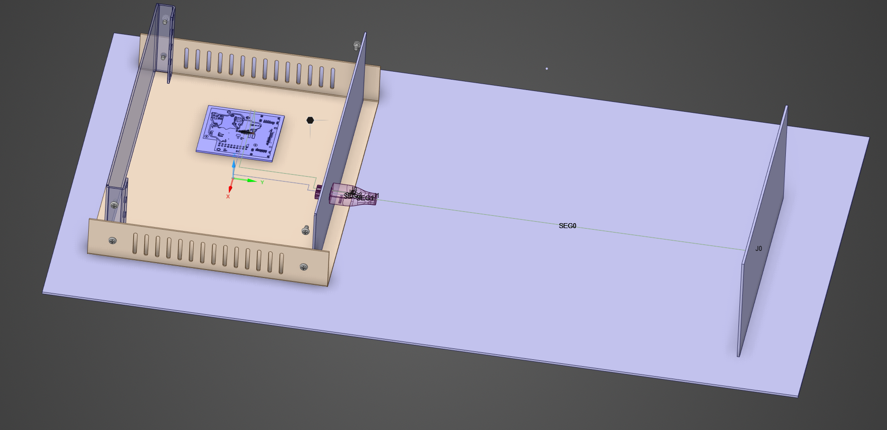
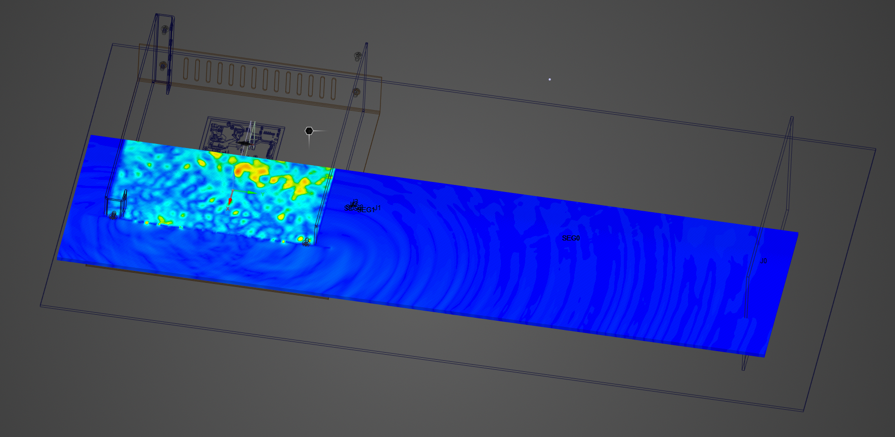
In this blog we will be using the ANSYS EMC Plus tool to simulate radiated emission of a PCB design placed inside an enclosure. The model also include an MHARNESS cable routed through the enclosure and connected to the PCB.
The workflow includes the following steps:
- Importing a PCB file using the Ansys Electronics Database (EDB) format
- Defining and assigning material properties
- Assigning the excitation source
- Defining the simulation domain
- Creating the fields probes
- Meshing the model, and running the simulation
The video link below shows an illustration on how to do these steps in detail, and the model shown is available in the downloadable resources.
Downloadable Resources