Lightning is a hazardous electrostatic discharge event in which two electrically charged regions cause the instantaneous release of up to one gigajoule of energy. The lightning strike behaves like a short, massive pulse of current and can cause serious damage to structures and electronic devices. Lightning strikes can be divided into direct and indirect categories, where the indirect effects are due to induced energy coupled to objects in close proximity to the strike location. Indirect lightning strikes are more common for many electronic applications, and although the induced currents are smaller than a direct strike they can still pose significant issues. This post will highlight an example workflow for simulating the effects of an indirect lightning strike on a multi-layer printed circuit board using an Ansys HFSS and Circuit co-simulation.
Lightning waveforms exhibit a double exponential characteristic shape as shown below. Multiple strikes consisting of a series of smaller amplitude pulses also occur, but this example uses the first strike since it is always the most severe. Lightning waveform standards have been developed which define the rise time from 10% to 90% of the peak amplitude and decay time from the peak amplitude to 50% and can be used to model the lightning pulse in simulations. Example standards include MIL-STD-464 for defense applications and ANSI/IEEE C62.41 for power distribution applications.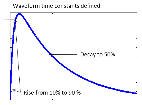
The effects of lightning strikes on electronic devices can be simulated using either the full-wave time-domain or frequency-domain finite element solvers in Ansys HFSS. This example uses the frequency-domain FEM solver combined with the time-domain Ansys circuit solver. The same approaches can be used for simulating the impact of electrostatic discharge (ESD) events on electronic devices according to standards such as IEC61000-4-2.
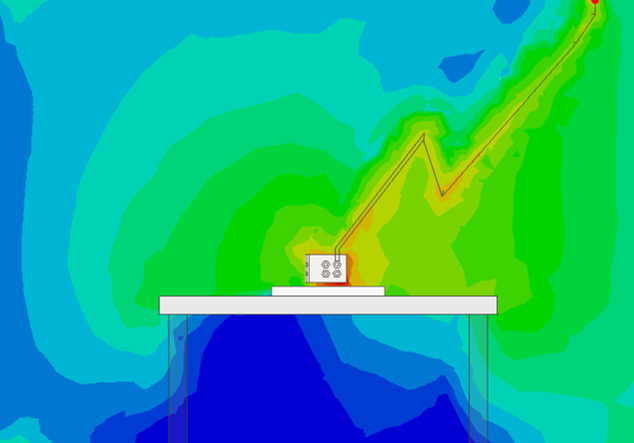
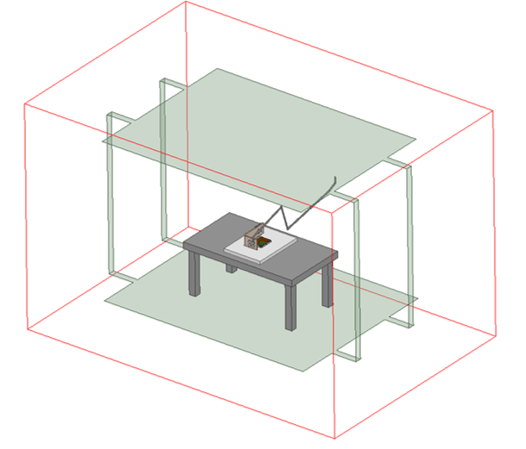
The simulation workflow for modeling currents induced in a PCB near a copper busbar which is struck by lightning is shown below. The HFSS model includes the multi-layer PCB, copper busbar structure, and aluminum platform and table. Variables may be assigned to automate studies of parameters of interest such as the separation distance between the PCB and busbar. Material properties, boundary conditions, and excitations are assigned to the model. The HFSS model is solved using a frequency sweep up to 50 MHz and dynamically linked into a circuit schematic also located within the Ansys Electronics Desktop environment. The dynamic link provides the S-parameters from the HFSS solution for use in the circuit model. A lightning waveform with a peak amplitude of 50 kA is used as the circuit current source excitation. The currents and voltages induced on the PCB conductors are available from the circuit simulation results and the bi-directional dynamic link enables the electromagnetic fields to be examined in the HFSS model.
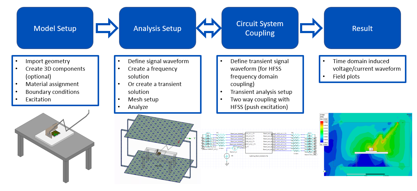
Rectangular lumped ports are assigned to model the lightning excitation and to the PCB locations where the induced effects from the strike are to be determined. An absorbing radiation boundary is assigned to the external faces of the surrounding air region. A pair of connected conducting plates serves as the lightning return path, and a conducting path connects the upper lightning port to the location of the strike on the busbar structure.
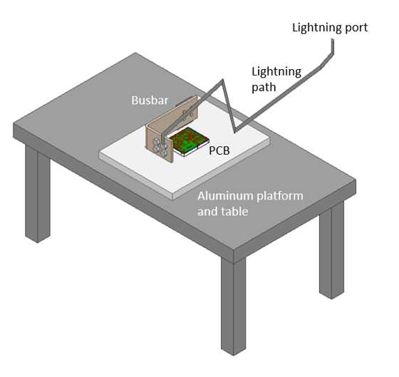
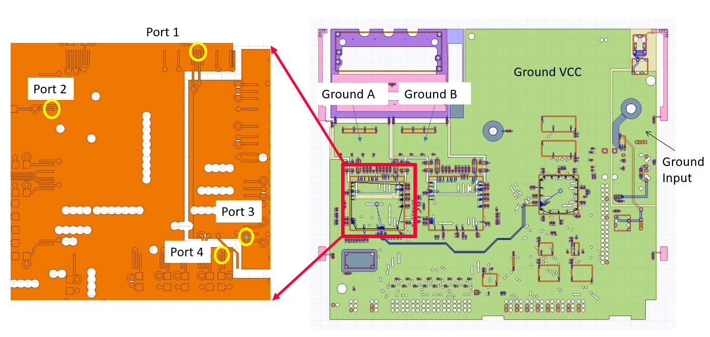
The PCB ports are placed on larger conductors of the multi-layer PCB which are expected to have higher coupling to the energy from the nearby lightning strike. In this example, these conductors are power planes which connect to sensitive electronic components which could suffer damage. The HFSS model uses the Driven Terminal solution type. The size of the PCB is approximately 170 mm by 200 mm and is located approximately 100 mm from the busbar structure.
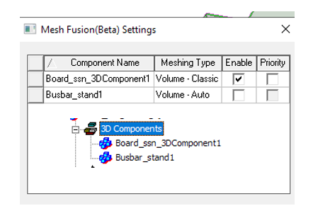
3D Components are used in the HFSS model to reuse ready-made objects such as PCBs, connectors, or the busbar structure. This also allows the use of Mesh Fusion which significantly increases the size of models that can be solved with the finite element method by applying the optimal meshing type to each 3D Component.
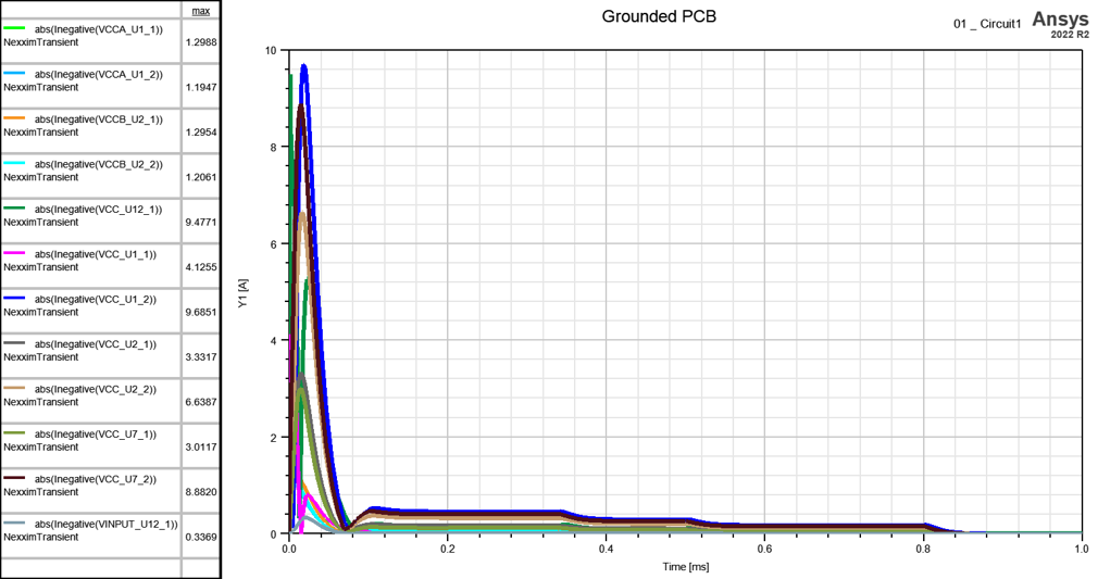
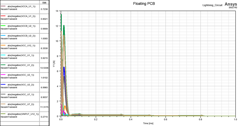
 The simulation results can be used to determine the impact of different PCB grounding connections on the induced currents and optimize the design for protection of sensitive components. In this example, transient current amplitudes of up to 10 Amps are observed in the PCB conductors. Updates to the HFSS model are easily passed through the dynamic link to the circuit simulation to determine the impact on the outputs of interest. The electromagnetic fields can also be examined to understand how to mitigate the near-field coupling to the PCB.