
SIwave is a power integrity and signals integrity tool. The signal net-analyzer solver is one of the tools in SIwave and will be discussed in this video.
EMI scanner is a fast scanning of the layout of the PCB. It looks for major design defects that could cause SI, PI, or EMI issues. This scanner is the first thing a designer needs to do when uploading a new mechanical design.
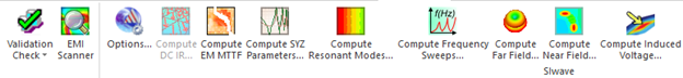
Figure 1: EMI Scanner
SIwave should not be used to build PCBs. While this is possible, it is not the best way to utilize SIwave. But instead, try to import files from professional CAD files. SIwave can import the following types of CAD files:
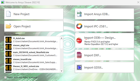
Figure 2: Import files
Any process in SIwave starts by selecting the solver. Once you select a solver, a dialog box pops up, and all the user needs to do is fill up the form and submit it.
So we select the EMI scanner to get this dialog box.
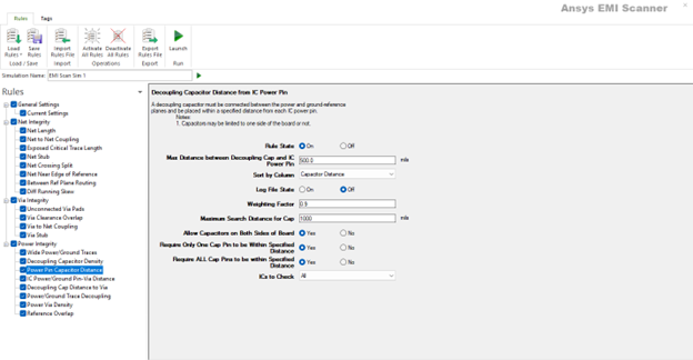
Figure 3: EM and SI rules
There are default rules for every kind of dimension and relation. The user can modify any of these rules. These rules simply mean that if the dimensions are smaller/bigger than the spec, there is a high probability of issues occurring in your design.
The user can import tools, activate rules, and deactivate rules. The user can also export tools for future use.
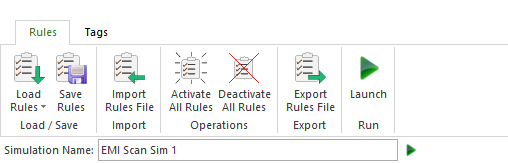
Figure 4: Import/Export rules
There are a few types that a user needs to know about.
SI rules
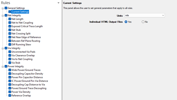
Figure 5: SI rules
EM rules
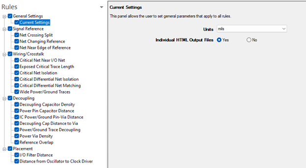
Figure 6: EM rules
Frequency-dependent EMI rules
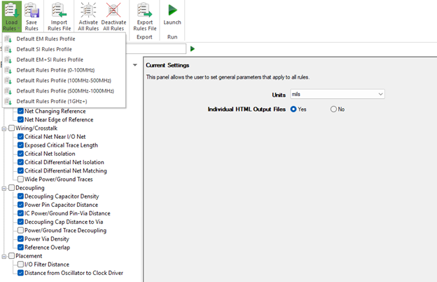
Figure 7: EM rules – Frequency dependent
After the scanning, the user can display the report.
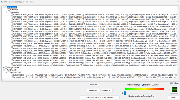
Figure 8: Warning list
Click on any line to see a description at the bottom of the rule. SIwave will also zoom in on the location of the problem.
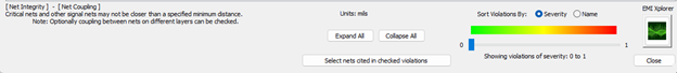
Figure 9: Description of the violations
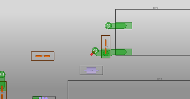
Figure 10: Location of the violation
If you want more, click on the EMI scanning to see a visual description of the issue, in addition to a signal analysis and damage due to the violation. For some rules, there will be nothing to show. Notice the signal analysis that it displays the default and the violation results. The user can add more options and see the impact on the signals. The plots can come in many different forms, depends on the rules. They could be in impedance, current, or voltage form.
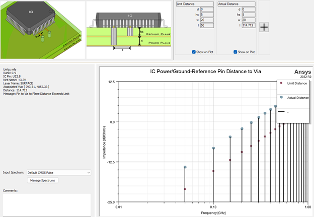
Figure 11: Detail description of the phenomena
Let us zoom in on these rules and see what we can conclude from them:
List of rules:
- Net Crossing Split
- Net Changing Reference
- Net Near Edge of Reference
- Critical Net Near I/O Net
- Exposed Critical Trace Length
- Critical Net Solution
- Critical Differential Net Isolation
- Critical Differential Net Matching
- Wide Power/Ground Traces
- Decoupling Capacitor Density
- IC Power/Ground-Reference Pin distance to via
- Decoupling Capacitor Distance to Via
- Decoupling Capacitor distance from IC power pin
- Power/Ground Trace decoupling
- Power Via Density
- Reference overlap
- I/O Filter distance
- Distance from oscillator to clock driver
- Net Length
- Net to Net Coupling
- Net Sub
- Between ref Plane Routing
- Diff Running Skew
- Unconnected Via Pads
- Via Clearance Overlap
- Via to Net Coupling
- Via Stub
C:\Program Files\AnsysEM\v231\Win64\config\EMIScanner\ViolationAnalyzerImages
Net crossing split
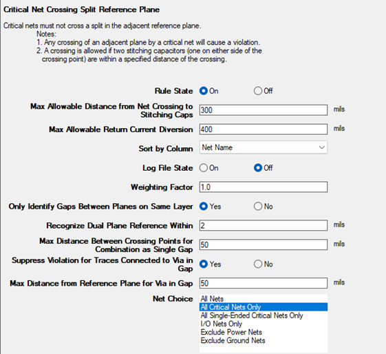
Figure 12: Form
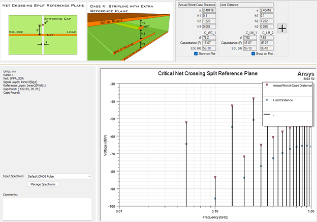
Figure 13: Result
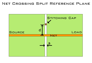
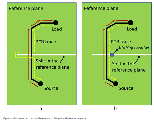
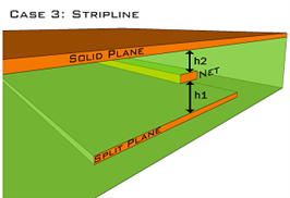
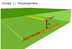
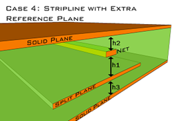
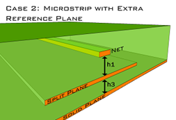
Figure 14: Models
https://www.ansys.com/blog/pcb-design-rules
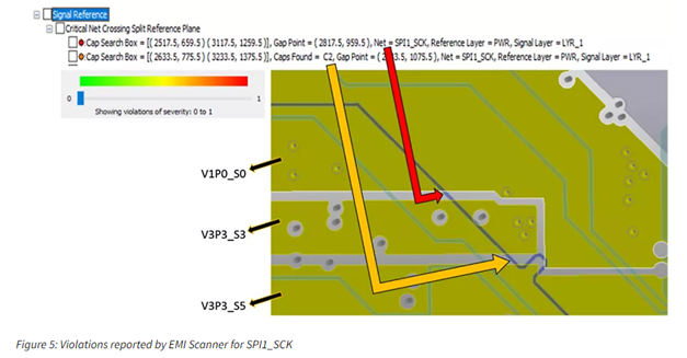
Figure 15: Example
Net changing reference
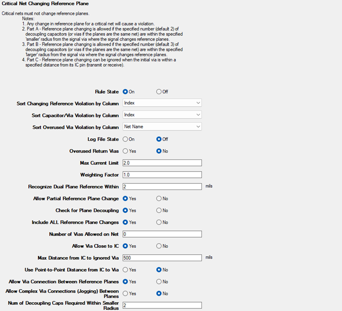
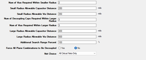
Figure 16: Form
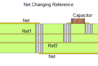
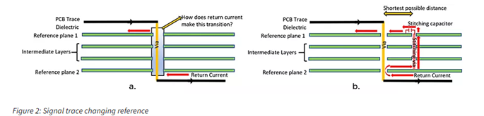
Figure 17: Models
Net near edge of reference
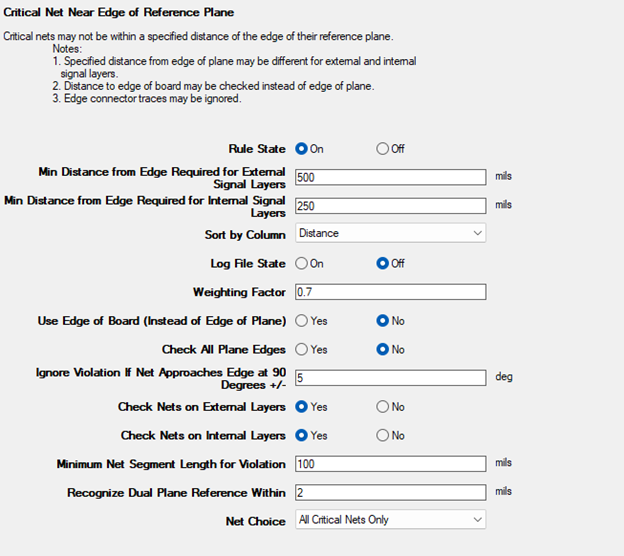
Figure 18: Form
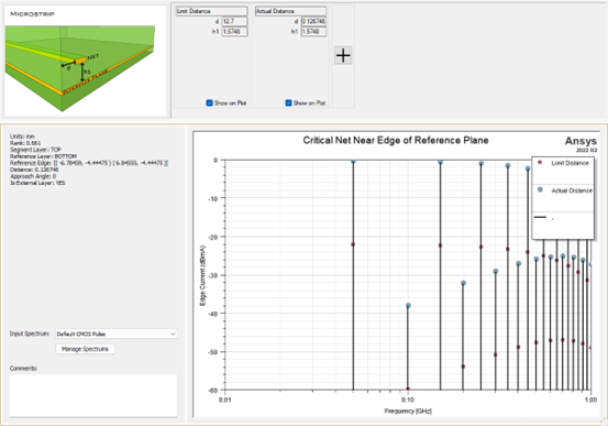
Figure 19: Result
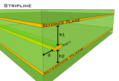
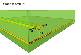
Figure 20: Models
Critical net near I/O net
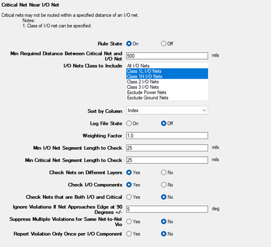 Figure 21: Form
https://www.ansys.com/blog/pcb-design-rules-wiring-and-crosstalk
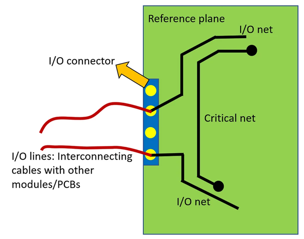
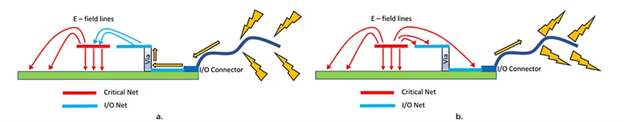
Figure 22: Models
Exposed critical trace length
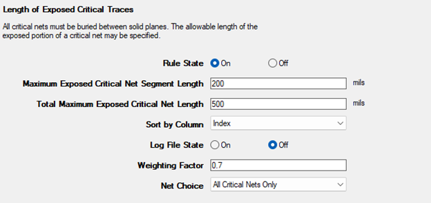
Figure 23: Form
https://www.ansys.com/blog/pcb-design-rules-wiring-and-crosstalk
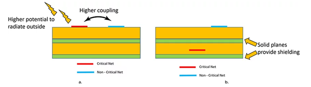
Figure 24: Models
Critical net isolation
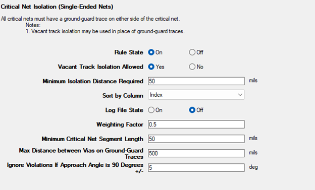
Figure 25: Form
Critical differential net isolation
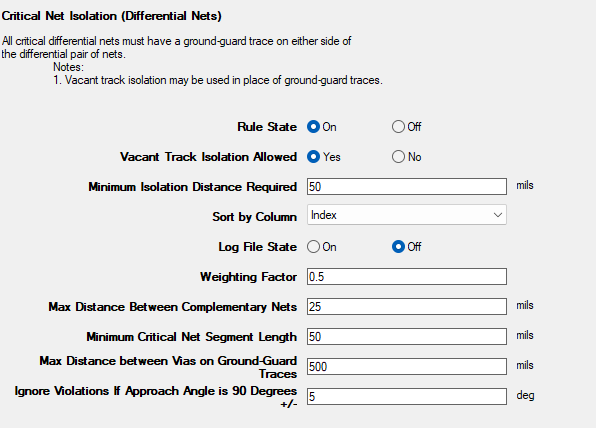
Figure 26: Form
Critical differential net matching
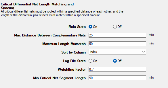
Figure 27: Form
https://www.ansys.com/blog/pcb-design-rules-wiring-and-crosstalk
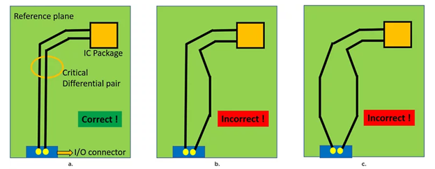
Figure 28: Models
Wide power/ground traces
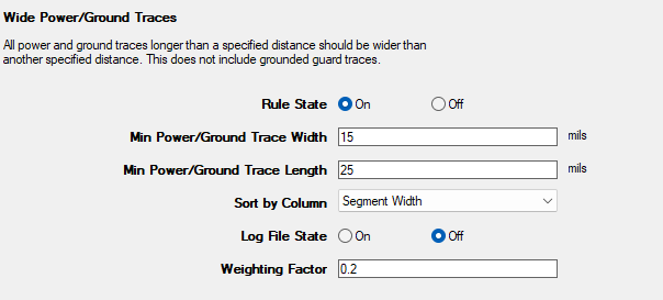
Figure 29: Form
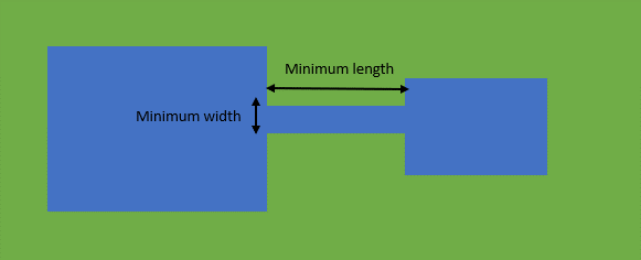
Figure 30: Models
Decoupling capacitor density
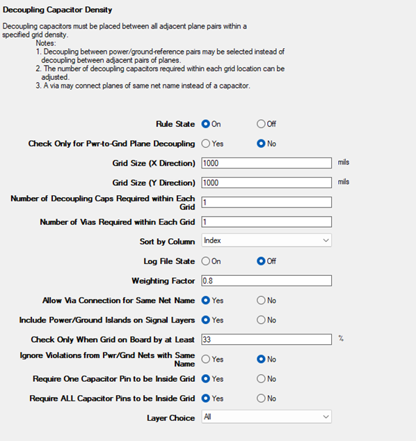
Figure 31: Form
IC Power/Ground-Reference pin distance to via2
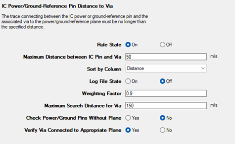
Figure 32: Form
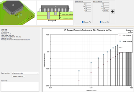
Figure 33: Result
Figure 34: Models
https://harrisburg.psu.edu/files/pdf/16506/2019/04/24/ansys_penn_state_si_symp_2019_final.pdf
Decoupling capacitor distance to via2
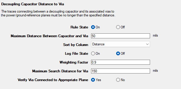
Figure 35: Form
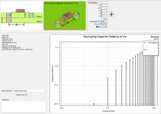
Figure 36: Result
p_2019_final.pdf
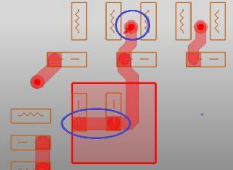
Figure 37: Model
Decoupling capacitor distance from IC power pin (Power pin capacitor distance)
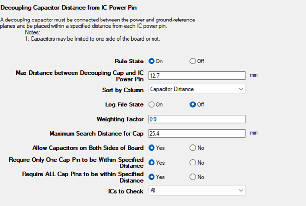 Figure 38: Form
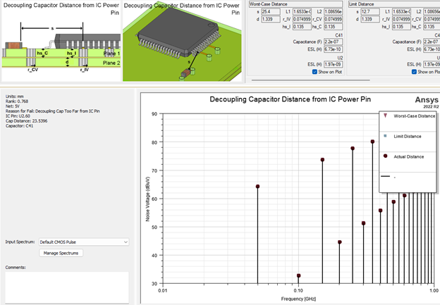
Figure 39: Result
You can enter Normalized, square or CMOS pulse signal
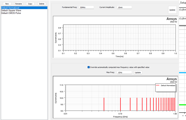
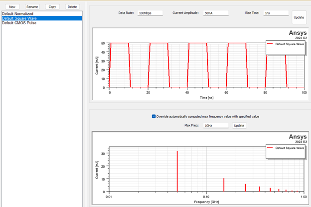
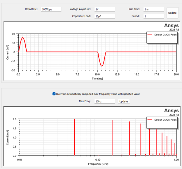
Figure 40: Signals
Power/Ground trace decoupling
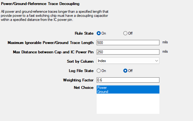
Figure 41: Form
Power via density
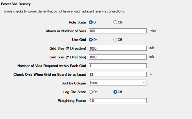
Figure 42: Form
Reference overlap
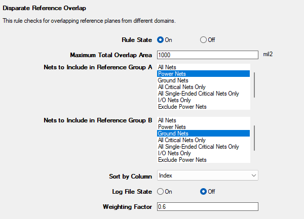
Figure 43: Form
I/O filter distance
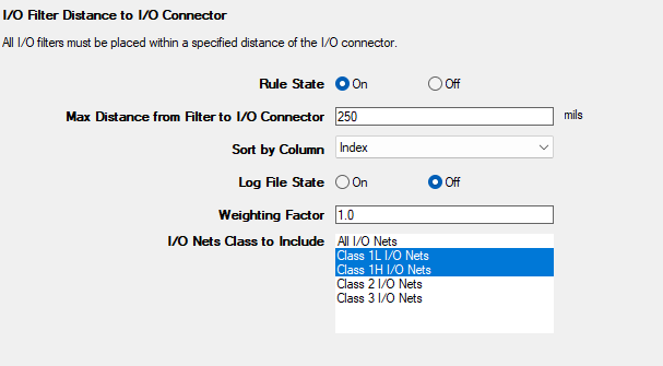
Figure 44: Form
Distance from oscillator to clock driver
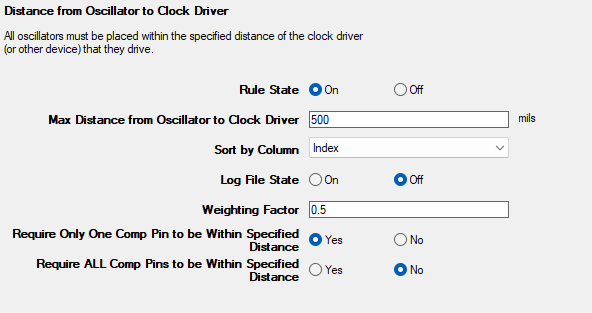
Figure 45: Form
Net length
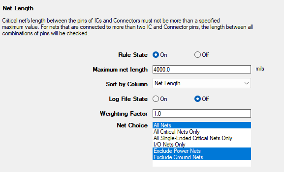
Figure 46: Form
Net to net coupling
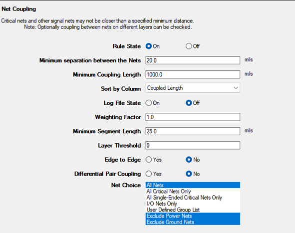
Figure 47: Form
https://harrisburg.psu.edu/files/pdf/16506/2019/04/24/ansys_penn_state_si_symp_2019_final.pdf
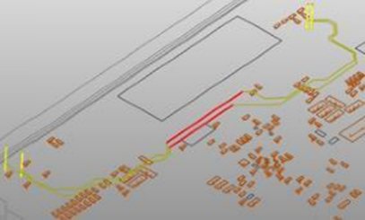
Figure 48: Model
Net sub
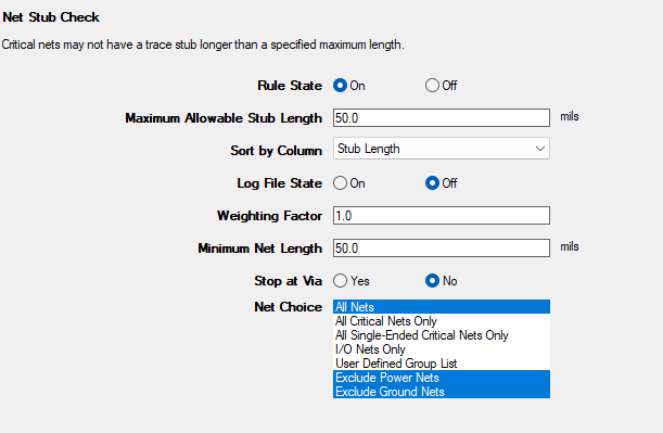
Figure 49: Form
Between ref plane routing
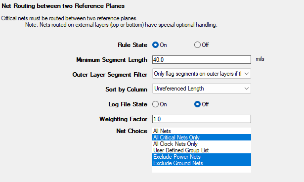
Figure 50: Form
Diff running skew
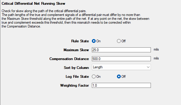
Figure 51: Form
Unconnected via pads
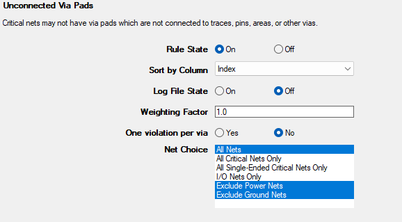 Figure 52: Form
Via clearance overlap
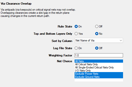 Figure 53: Form
Via to net coupling
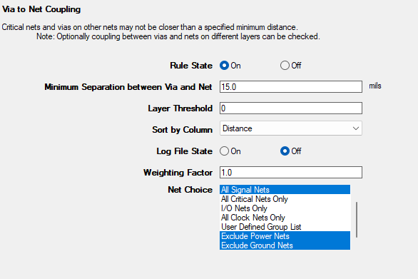 Figure 54: Form
Via stub
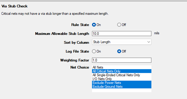 Figure 55: Form
https://harrisburg.psu.edu/files/pdf/16506/2019/04/24/ansys_penn_state_si_symp_2019_final.pdf
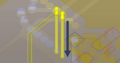
Figure 56: Model
