
SIwave is a power integrity and signals integrity tool. An induced voltage solver is one of the tools in SIwave and will be discussed in this video.
An induced voltage solver measures if the PCB is shielded against any noisy signal from external sources. It calculates the noise voltage on any port in the model. But if the PCB accepts noise, then it can also radiate.
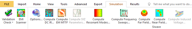
Figure 1: Compute Induced Voltage
SIwave should not be used to build PCBs. While this is possible, it is not the best way to utilize SIwave. But rather try to import files from professional CAD files. Siwave can import the following type of CAD files:
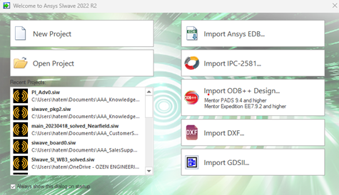
Figure 2: Import files
Any process in SIwave starts by selecting the solver. Once a solver is selected, a dialog box pops up, and all the user needs to do is to fill up the form and submit it.
However, some solvers require ports before one can select the solver. The induced voltage solver expects ports in the model; otherwise, it will not be activated.
To create ports, there are many ways:
- When uploading all the design, SIwave shows a list of all the nets and ask the user to assign ports to the nets.
- The second way, to create ports on the power planes, use the PI solver to do that without launching the PI solver.
- The third way for traces and also power planes, one can assign ports using Tools and generate ports on selected nets. Same thing here, select the traces, then click generate ports. When any trace is selected, SIwave only shows the pins of the last trace. That does not mean that the previous ones are not selected.
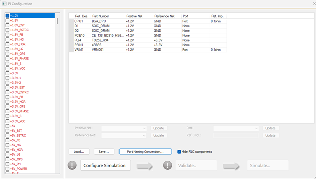
Figure 3: PI port assignment
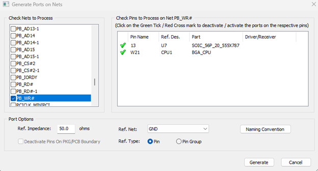
Figure 4: Assign ports to nets
Next step, specify the frequency band. One can have multi-bands for that. Then specify the incident wave. Use the spherical or the cartesian coordinates. It is easy to explain it with the Cartesian.
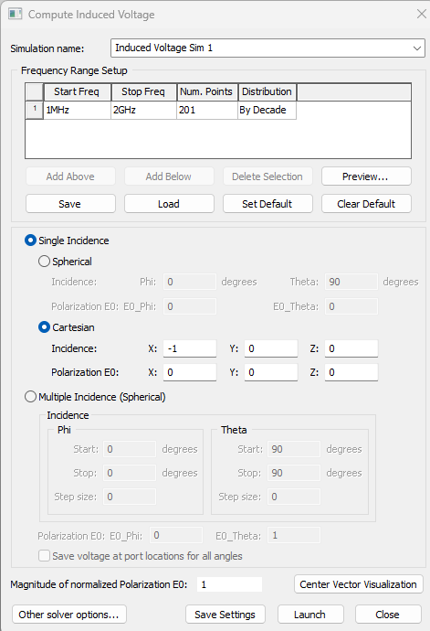
Figure 5: Compute Induced Voltage dialog box
Select the direction of the wave to be negative X, it means that the wave is coming from the positive towards the negative x. if positive X, it means that the wave is coming from the negative towards the positive x. Click on the Center Vector Visualization to see the vectors. Rotate to see in 3D.
Select -Z, the waves then come from the top, down to the PCB, and +Z comes from the bottom of the PCB going up.
Same thing with spherical. One needs to specify both angles, the Theta and the Phi. Having Theta 90 degrees means it is in the X-Y plane, then select Phi 45.
After selecting the direction of the wave, the user needs to specify the polarization. Usually, the polarization is in the perpendicular plane. So if it is X =-1, the polarization will be in the Y-Z plane. And the same thing, rotate the plot in 3D to see the polarization. So -1 is going from the top to the bottom. That is the polarization direction.
One can also have multiple incidences, i.e., waves coming from many directions. In this case, specify a Phi and Theta values range with the step size. Then ask SIwave to save the voltage at each port for each case. The polarization is defined using one entry and not one for each direction. So the wave is coming from the +x to -x, and the Theta and Phi numbers are the way the board is being rotated.
The last thing the user needs to do is to specify the magnitude of the wave in V/m
Change the solver setup by clicking on the Other solver option. Select to go with balanced or fast, or optimum accuracy. Start with Balanced, and if it took a short time, change it to the optimum accuracy.
Now solve
Examining the solution:- Plot the voltage noise at each port in the model.
Select to see the results to get the following dialog box. Select to display the voltage on all or some of the ports.
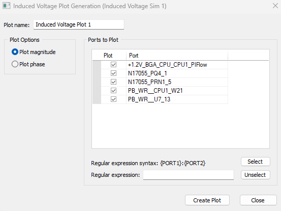
Figure 6: Select the nets to examine.
The result is a simple plot showing a graph of the voltage noise at each port along the band of interest. This plot shows which port is more sensitive and over which band. If that band is essential, the user must modify the design.
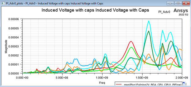
Figure 7: The voltage noise at each port
Add a limit line. This way this graph can be used in any presentation. Then immediately SIwave will display a column showing any violation.
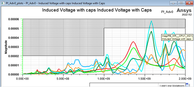
Figure 8: The voltage noise with the limit line
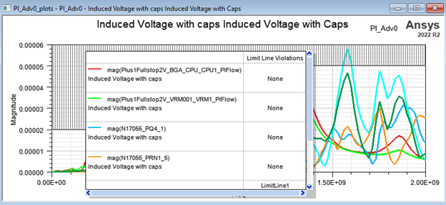
Figure 9: The voltage noise showing violations in the table.
Add markers on any curve to read the voltage at a port at a specific frequency. Also, right-click, select trace characteristics, then select a function. For example, select the max and the min. The user can change the precision by double-clicking on any column. Then in the properties, change the field width and the precision.
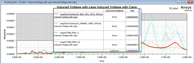
Figure 10: The voltage noise showing the maximum of each curve.
Let us look at the results of the power plane. The red line is the response using decoupling caps. So what happens if the decoupling caps are removed? So I deactivate the decoupling caps and g Home, Circuit Element Parameters. Then rerun the induced voltage solver. The results show how the decoupling caps can suppress the capability of the powerplane to detect and accept the noise. And that is another reason for using the decoupling caps.
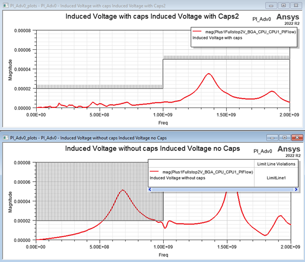
Figure 11: Comparison between the amount of noise with/without the decoupling caps
Repeat these calculations for each direction and each polarization, 2 by 6, 12 cases with and without decoupling caps. That will provide the user with a complete study of the susceptibility of the power planes to external noise.
Debug the solver:- Simulation Properties
One can examine the setup of the solver. This is good in the future to know the setup used to generate a solution. The setup cannot be changed to keep the history of the solution.
Figure 12: Solver setup
- Profile
The profile is another important means to examine the solution. It gives an idea of the solver timing and the mesh used in each net. This information is used to compare different models or even different solutions of the same model. The user can also use this information to plan long runs.
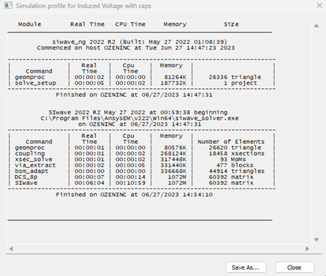
Figure 13: Profile of the solution
