
SIwave is a power integrity and signals integrity tool. Compute Frequency Sweeps is one of the tools in SIwave and is the subject of this blog.
Compute Frequency Sweeps solver is used to study resonance in power planes. Similar to the resonant mode solver discussed in another video, with a few differences. A frequency sweep solver detects resonant modes based on physical dimensions and the effect of the source and load. With the help of the circuit tool, the frequency sweeps solver injects the right voltage for each frequency based on the actual spectrum of the signal. As a result, the frequency sweeps solver can determine the magnitude of each resonance.
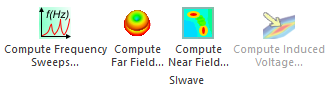
Figure 1: Compute Frequency Sweeps solver
Let us start.
It is not recommended to use SIwave to build PCBs. Although this is possible, it is not the best way to use SIwave. SIwave can import the following types of CAD files:
Figure 2: Import dialog box in SIwave
Ansys EDB translator can be installed on Allegro and Altium to produce EDB files. Orcad users are recommended to use IPC-2581. Mentor Expedition users should use ODB++ files. Cadence users should generate BRD files and import them into the 3D layout. This requires Cadence to be installed, Extracta from Cadence to be installed, and the path of Extracta from Cadence should be set in the Path environment variable.
SIwave extracts a lot of information from the CAD file, including the stackup, materials, components, and nets. As a result, the model is ready for solving.
Adding sources.
After importing the model, the next step is to add sources. SIwave needs to know how and where each power plane net is excited. In SIwave, sources can be added in three ways: the DCIR setup or the net way, the manual way, or the component way.
DCIR setup
Click on the orange mini-icon at the top left corner of the screen.
Figure 3: Orange icon to access workflow wizard
And from the list, select the DC IR solver.
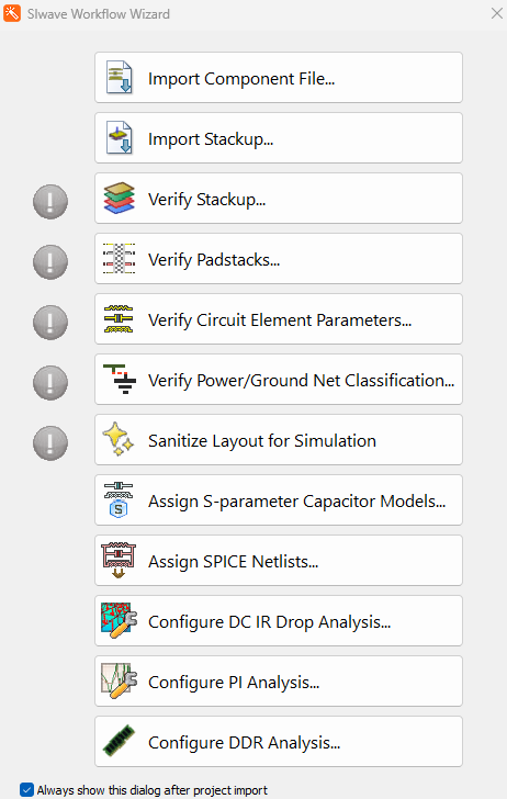
Figure 4: Workflow wizard
The DCIR setup dialog box appears after selecting the DCIR. Next, the user must choose a power plane or group of power planes and assign them voltage and current sources. The voltage sources are assigned at the input, while the current sources are usually on the load side (die side).
Understanding passive links in SIwave is essential before proceeding. It can be one net or many nets connected in series using passive components, such as capacitors, inductors, and resistors. Power planes normally use inductors and resistors but not capacitors.
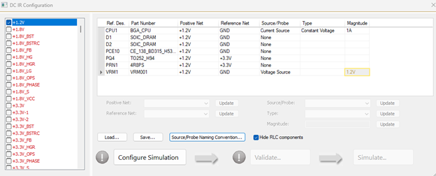
Figure 5: DCIR dialog box
Based on this configuration, at each frequency, the input voltage will be 1.2V and the input current will be 1A. Configure, validate, but no need to solve.
The new voltage and current sources can be found in the component panel.
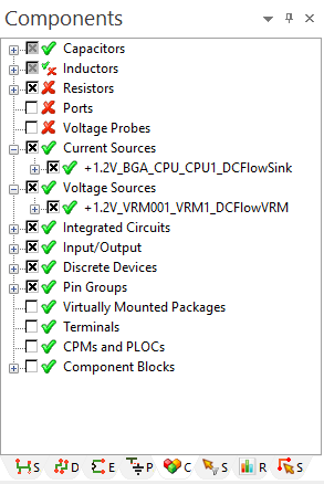
Figure 6: Components tab
In addition, they can be found in the Circuit Element Parameters from Home section.
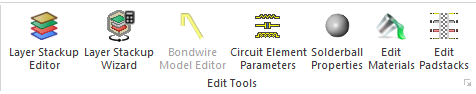
Figure 7: Circuit Element Parameters
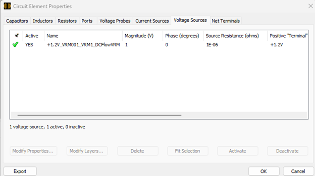
Figure 8: Circuit Element Panel
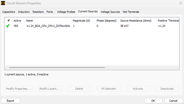
Figure 9: Circuit Element Panel
Manual way:
Manually assigning ports is another option. From Home, select the voltage source and the current source.
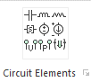
Figure 10: Circuit Element fast access icons
The user must know where the source is as well as where the nearest ground is. By selecting two points on the PCB, SIwave instantly recognizes all the nets under these two points. Any layer can be selected for the positive terminal and the negative terminal. Below, the positive and negative terminals are on the surface.
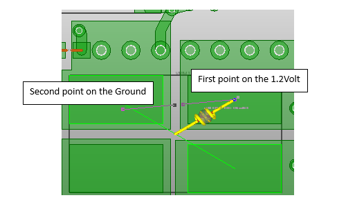
Figure 11: Manual way to add ports
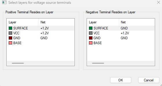
Figure 12: Define the layers of the terminals of the new port
Component way
Components are the third way to add ports. From Tools, select Generate Circuit Element on Components:

Figure 13: Tools-> Generate Circuit Element on Components
First, select the part name, then the reference designator, to select the component. Select a positive pin and a negative pin from the list, then select the voltage source or the current source from the Circuit type. When the component has many pins on a net, the user can define and use a group of pins. There are many videos discussing creating groups of pins.
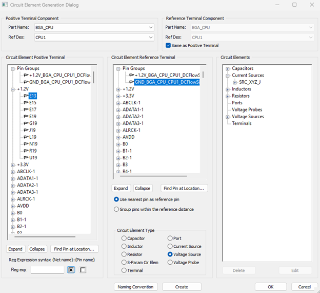
Figure 14: Adding elements by selecting components first
Setting up the Frequency Sweep solver
Click on the Compute Frequency Sweeps solver.
Give the solution a name.
Excitation option 1 uses the sources defined inside SIwave. A second option is to use an external source, which will be discussed next.
Choose the frequency band, in this case, 1MHz-2GHz, and request to plot the surface voltage difference between Vcc and GND.
After saving the settings, the user can launch the program.
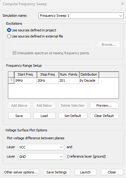
Figure 15: Solver setup
Solutions
View Profile
Another important way to examine a solution is through its profile. This shows the solver timing and mesh used in each net. Different models can be compared using this information. Long runs can also be planned using this information.
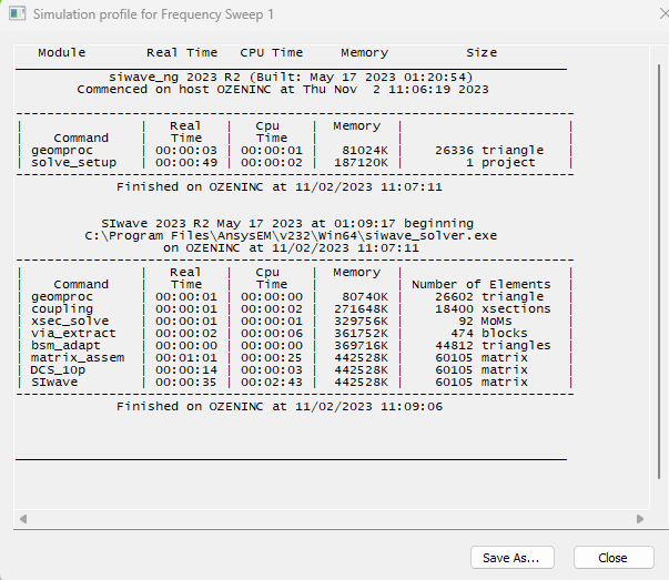
Figure 16: Profile panel
View Simulation Properties
View simulation properties can be used at any time to see the setup used to generate this solution.
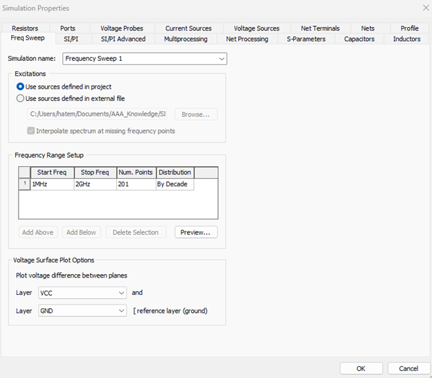
Figure 17: Old simulation setup
Plot Surface Fields
The field can be plotted at any frequency on the selected layer. It is also possible to animate through all the frequencies. The scale goes up to 2.19 Volts. Only 1.2 Volt is supplied to the power plane. This means that at certain frequencies, there are resonances. Run the animation and observe where the high values occur to detect these resonances. Using this information, the user can place voltage probes.
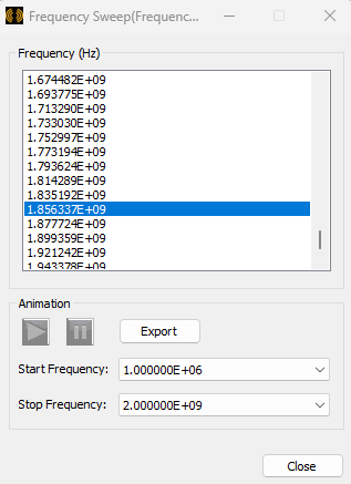
Figure 18: Frequency contents
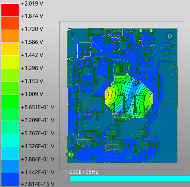
Figure 19: Field plot
Plot probe Voltages
Only three or four voltage probes should be added manually to the power plane. This is because the location of the voltage probe is not a pin and is not a connection between a net and a component.
From Home, select voltage probes.
Figure 20: Circuit Element Panel
Ensure that the positive terminal is on the VCC layer and the negative one is on the GND layer. In the setup, the user selected to plot the field difference between the VCC layer and the GND layer. Rerun the solution with probes.
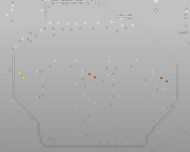
Figure 21: Add voltage probes
Based on these results, one can determine at what frequencies resonances occur. A frequency with a voltage above 1.2 Volt needs to be examined. There are reflections at many frequencies, especially at low frequencies, but they are not as severe as at 1.33GHz. Two others are weaker: 0.892GHz and 1.877GHz.
The assumption in these results is equal voltage amplitude and equal load current at all frequencies. Therefore, these results cannot be used to make decisions. The right signals must be injected to see the resonance. As a result, it is important to know the right spectrum of the signal.
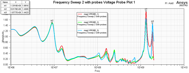
Figure 22: Probe results
Customized sources
AEDT's circuit tool allows one to inject the right voltages and currents. To use the circuit tool, SIwave must first solve the structure's S-parameters using the PI solver.
PI solver
Select the PI solver by calling the orange mini-icon in the top-left corner of the screen. Assign ports to the inputs and outputs of the Powerplane of interest.
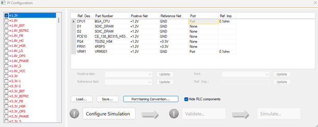
Figure 23: PI dialog box
Configure, validate, and simulate. Set the band in the solver setup. The circuit uses the transient solver, so don't forget to include 0Hz. It is important to note that the maximum frequency number affects the rising time number. 0.5/Freq is used to calculate the rising time.
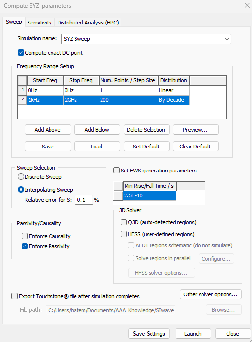
Figure 24: SYZ solver setup
Circuit Setup
Start the Ansys Electronic Desktop and create a new project. Save the project in the same directory as the SIwave model. Add a Circuit project. Then, add an SIwave link.
Figure 25: SIwave icon link in the circuit tool
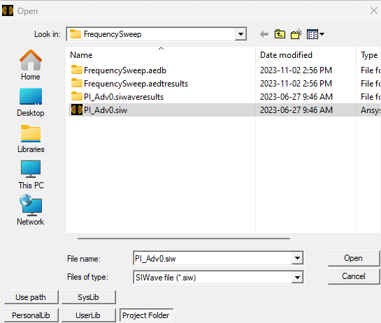
Figure 26: Assign the right SIwave file
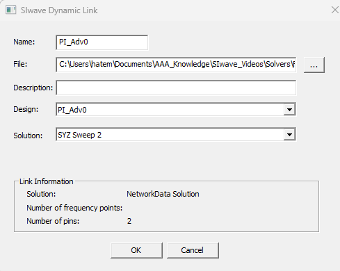
Figure 27: Select the right file and the right solution.
Add a resistor R=1Ohm on the CPU side and add a voltage (noise) source on the VRM side. From the independent sources, add a PRBS signal source with amplitude equal to 0.2Volt.
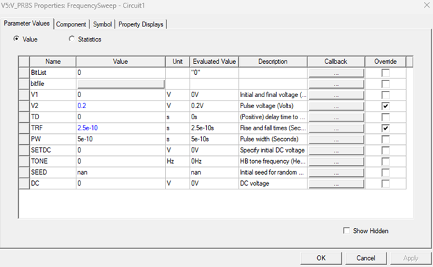
Figure 28: Adjust the entries of the voltage source
Add a transient solver with 0.1ps step and 100ns duration. The step is determined by the worst rising time, and the duration should be long enough to capture the spectrum of the noise signal. It may be necessary to try different lengths.
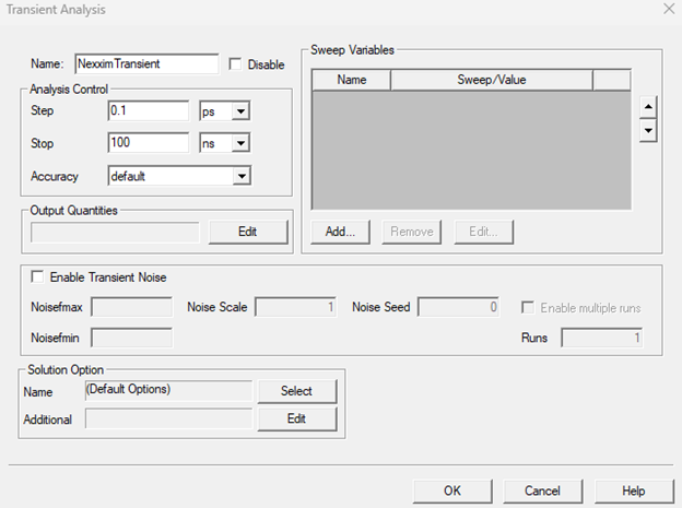
Figure 29: Transient solver setup
Using the solution, the user can plot the voltage and current on any trace. Many bits should be visible to the user. The more data, the more accurate the analysis.
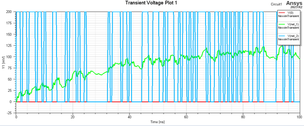
Figure 30: The voltage on all the nets of the circuit (Input, Output and ground)
The user can also plot the spectrum contents of the signal. When creating a standard report, select the spectral option: Create Standard report-> Rectangular plot-> Domain: spectral. This explains why the user must solve for many bits. Spectrums become more accurate as more bits are added.
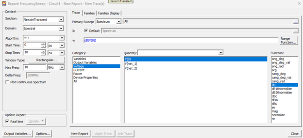
Figure 31: Plot the input signal spectrum
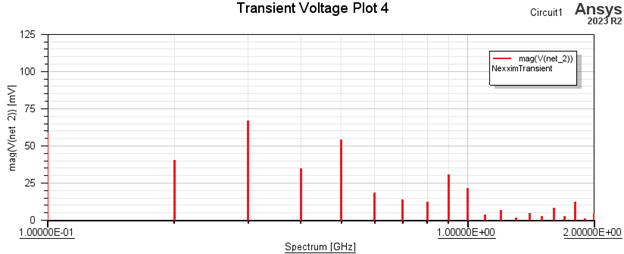
Figure 32: The input signal spectrum
Push the setup to SIwave using the Push Excitation option.
Figure 33: Push excitation
Back to SIwave
Launch the frequency sweeps again in SIwave. The solver is choosing to use external data instead of internal data.
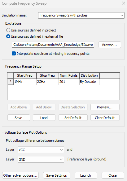
Figure 34: Use external source.
Launching the solver with the same setup. The voltage at the three voltage probes can now be plotted again. Note the input spectrum of the source (bottom) and the sweeping response (top). At 1.3GHz, there is a serious resonance.
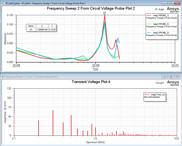
Figure 35: Resonance versus input spectrum
Plot the field at 1.3GHz. One can see the resonance location.
.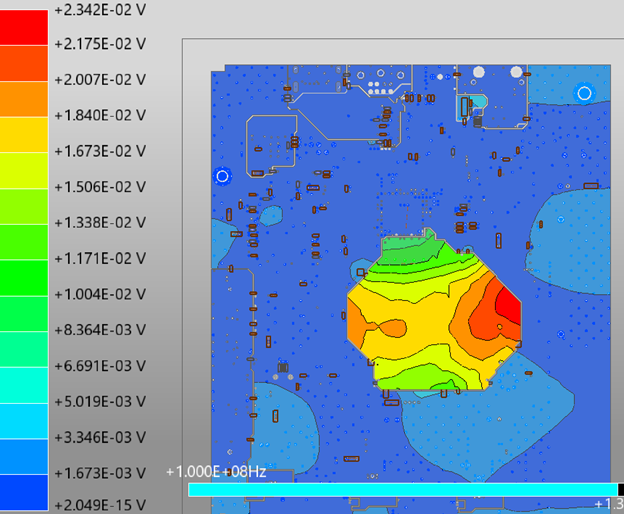
Figure 36: Field plot of 1.3GHz resonance
Resonant mode solver
Resonant mode solvers calculate resonances based on physical structure. It is important to compare the results from the frequency resonance solver with those from the frequency sweep solver. Another video explained the resonant mode. It is only the results that will be discussed in this article.
The resonant mode solver provides a list of resonances. To find the critical ones, the user must scroll through them one by one. The resonant mode solver detects resonance at 1.2875GHz. Due to the fact that the injected signal only has a component at 1.3GHz, what the frequency sweeps solver sees are the sides of the resonance, not the maximum.
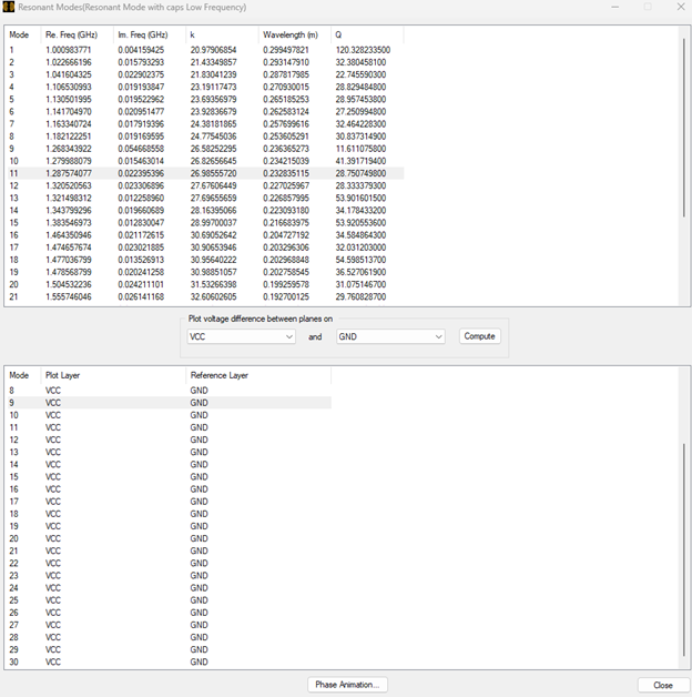
Figure 35: List of resonances
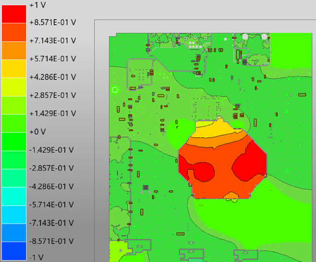
Figure 38: Field plot of resonance at 1.287GHz
Conclusion
Using the frequency sweeps solver is much easier than using the resonant mode solver to find resonances. The resonances detected by frequency sweeps using a custom source are more accurate than those detected by any other tool.
